In-cell touch display device

Active Publication Date: 2014-06-26
SHANGHAI TIANMA MICRO ELECTRONICS CO LTD
View PDF4 Cites 27 Cited by
  • Summary
  • Abstract
  • Description
  • Claims
  • Application Information

AI Technical Summary

Benefits of technology

The patent describes a new design for metal grids in touch layer structures for electronic devices. The metal grids are designed with larger densities at the edges and smaller densities in the center, which reduces resistance and mutual capacitance between neighboring metal grids. This design also makes the metal grids invisible in the display, as they are shielded by a black matrix layer. The resulting touch layer has lower resistance and improved performance compared to traditional touch layers made of ITO.

Problems solved by technology

That is, to prepare a touch display screen, a display device and a touch panel are prepared separately and then assembled to form the touch display device, which results in a relatively high cost and a bulk display screen and does not meet the present needs for a light-weight and thin display device.
In the prior art, although the parasitic capacitance caused by the output lead wires of the touch structure layer is decreased by shielding the output lead wires, the parasitic capacitance between the drive electrodes and the sense electrodes in the touch structure layer and the display device also significantly impacts the touch effect.
In the touch liquid crystal display device, the touch layer is close to the conductive layers such as the pixel electrodes, the data lines and the scan lines on the array substrate, causing very large parasitic capacitances that are disadvantageous for the detection of a touch signal.
Therefore, as for the touch liquid crystal display device, many problems such as decreasing the resistance and parasitic capacitance, improving light transmittance, and improving the display effect need to be solved.
Besides, if the size and the resolution of the touch panel are increased, more electrodes and lead wires are required and the above problems get more severe.

Method used


Image

  • In-cell touch display device
  • In-cell touch display device
  • In-cell touch display device

Examples


first embodiment

A First Embodiment

[0022]A liquid crystal display device with a built-in touch panel is provided in the first embodiment. A schematic structural view of the liquid crystal display device is shown in FIG. 3. As shown, the liquid crystal display device include a color filter substrate, an array substrate 9, as well as a liquid crystal layer 8 and an organic layer 5 both disposed between the color filter substrate and the array substrate 9. The organic layer 5 is used as a protective layer. The color filter substrate includes a substrate 1 which is a glass substrate, a black matrix layer 2, a color filter layer 3, and a touch layer 4.

[0023]The top view of the black matrix layer is shown in FIG. 4. The black matrix layer 2 is constituted by an intersectional grid and is made of a common material, such as, chromium. As known by those skilled in this art, FIG. 4 shows only a portion of but not all of the black matrix layer on the substrate, and various modifications can be made to the shap...

second embodiment

A Second Embodiment

[0035]In an in-cell touch display device provided in the second embodiment, in the metal grid electrodes, the density of the metal grid electrodes decreases gradually from the edge direction of the metal grid electrodes to the center direction of the metal grid electrodes.

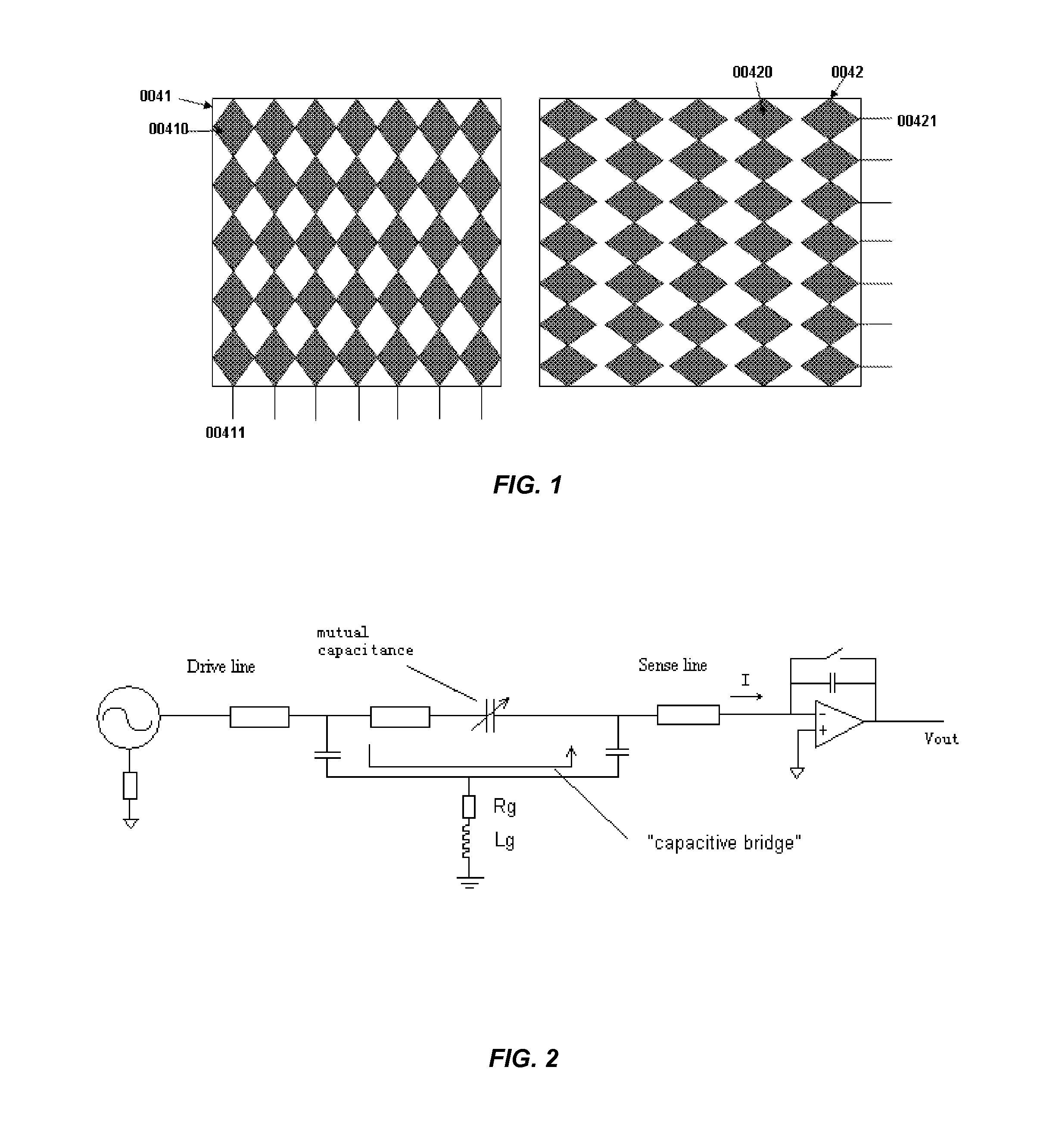
[0036]FIG. 8 is an exemplary structural view of a preferred embodiment of a touch unit. As shown, the touch layer includes drive electrodes A1 and A2, as well as sense electrodes B1 and B2. The drive electrodes A1 and A2, and the sense electrodes B1 and B2 which compose one pixel structure of the touch layer are arranged adjacent to each other and made of metal grid electrodes. In the light transmission direction, projections of metal grid electrodes fall within the projection of the color filter of the black matrix. The color filter comprises a plurality of sub-pixel 300.

[0037]At a place adjacent to the edge direction of the metal grid electrode, the density of the metal grids is the maximal. Fo...


PUM


Abstract

An in-cell touch display device is disclosed. The device includes a color filter substrate, a Thin Film Transistor array substrate, and a liquid crystal layer disposed between the color filter substrate and the Thin Film Transistor array substrate. The color filter substrate includes a grid black matrix layer, a touch layer, and a color filter layer, where the touch layer includes a plurality of metal grid electrodes. In addition, each electrode is aligned with the grid of the black matrix layer in a light transmission direction, and a density of the metal grid electrodes adjacent to the edge of the metal grid electrodes is greater than a density of the metal grid electrodes adjacent to the center of metal grid electrodes.

Description

CROSS-REFERENCES TO RELATED APPLICATIONS[0001]The present application claims the benefit of priority to Chinese patent application No. 201210573130.5, entitled “IN-CELL TOUCH DISPLAY DEVICE”, filed with the Chinese Patent Office on Dec. 25, 2012, the contents of which is incorporated herein by reference in its entirety.TECHNICAL FIELD[0002]The present invention relates to touch technologies, and in particular to a liquid crystal display device with a built-in touch panel.BACKGROUND OF THE INVENTION[0003]A touch display screen is one of important carriers which integrates an input terminal and an output terminal. In recent years, the market demand for touch display screens is boosting alone with the emergence of series of compact light-weight handheld devices such the iPhone. Previous touch display screens each are realized by superposing a touch panel on a display screen. That is, to prepare a touch display screen, a display device and a touch panel are prepared separately and then ...

Claims


Application Information

Patent Timeline
IPC IPC(8): G06F3/044G09G3/36
CPCG06F3/0412G06F3/0443G06F3/0446G09G3/36
Inventor ZHOU, XINGYAOYAO, QIJUNWANG, LIHUA
Owner SHANGHAI TIANMA MICRO ELECTRONICS CO LTD
Why Eureka
Try Eureka