
LED package structure, dam structure thereof, and method of manufacturing LED package thereof

a technology of led package and dam structure, which is applied in the direction of semiconductor/solid-state device manufacturing, electrical equipment, semiconductor devices, etc., can solve the problems of increased production cost, defective appearance, and insufficient flexibility of conventional dam construction formed by molding method, so as to reduce the possibility of wire pressing, improve the uneven appearance, and increase the height ratio

Inactive Publication Date: 2014-06-26
LITE ON ELECTRONICS (GUANGZHOU) LTD +1
View PDF2 Cites 16 Cited by
  • Summary
  • Abstract
  • Description
  • Claims
  • Application Information

AI Technical Summary

Benefits of technology

The present patent provides an LED package structure that improves the uneven appearance of conventional dam structures. The structure has a greater ratio of height to width, reducing the possibility of wires being pressed over and increasing the light emitting area. The method of manufacturing reduces production cost and increases the overall yield rate of the LED package structure. The bi-layered dam structure creates more space on the carrier to accommodate more LED chips.

Problems solved by technology

It results in an increase in production cost.
Therefore, conventional dam construction formed by molding method does not have enough flexibility when the contour of the dam structure needs to be redesigned.
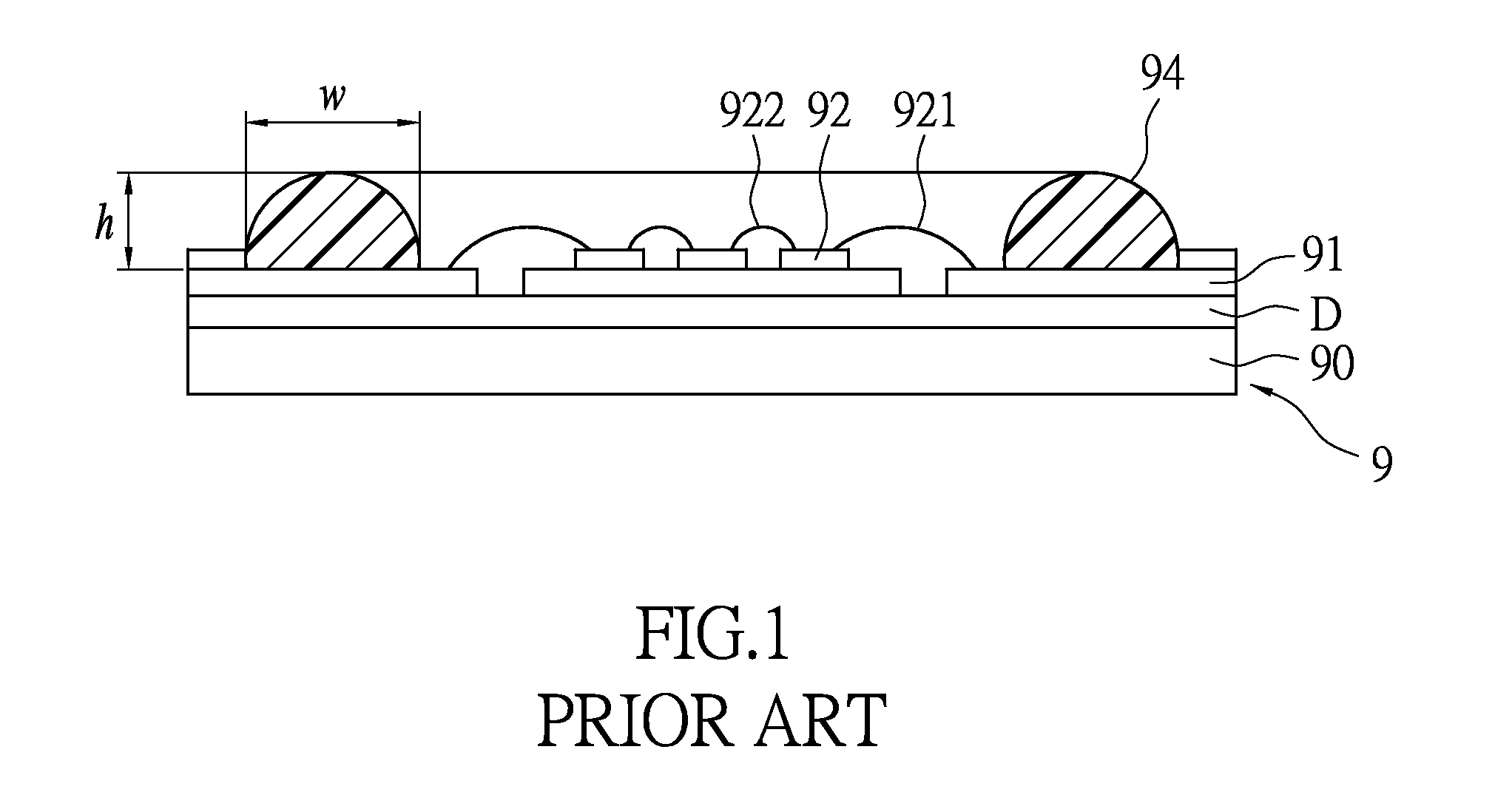
This dispensing method often results in defective appearances of the dam structure 94, especially at the starting and ending portions which are prone to protuberances, often leading to the unevenness of the glue surface.
The unevenness of the glue surface may further result in the color consistence when the light emitted from the LED chips 92 passes through the unevenness of glue surface.
Therefore, shape inconsistency of the dam structure is a concern in mass production.
Additionally, the wire is likely to be pressed by the fat and wide dam structure 94 such that wire malfunction is occurred.
Therefore, when the outer diameter of the dam is too large, the number of LED chips that can be placed within the light-emitting area will be affected, and the optical lens with standard scale cannot engage with all kinds of the dam structures having different outer diameter.

Method used


Image

  • LED package structure, dam structure thereof, and method of manufacturing LED package thereof
  • LED package structure, dam structure thereof, and method of manufacturing LED package thereof
  • LED package structure, dam structure thereof, and method of manufacturing LED package thereof

Examples


first embodiment

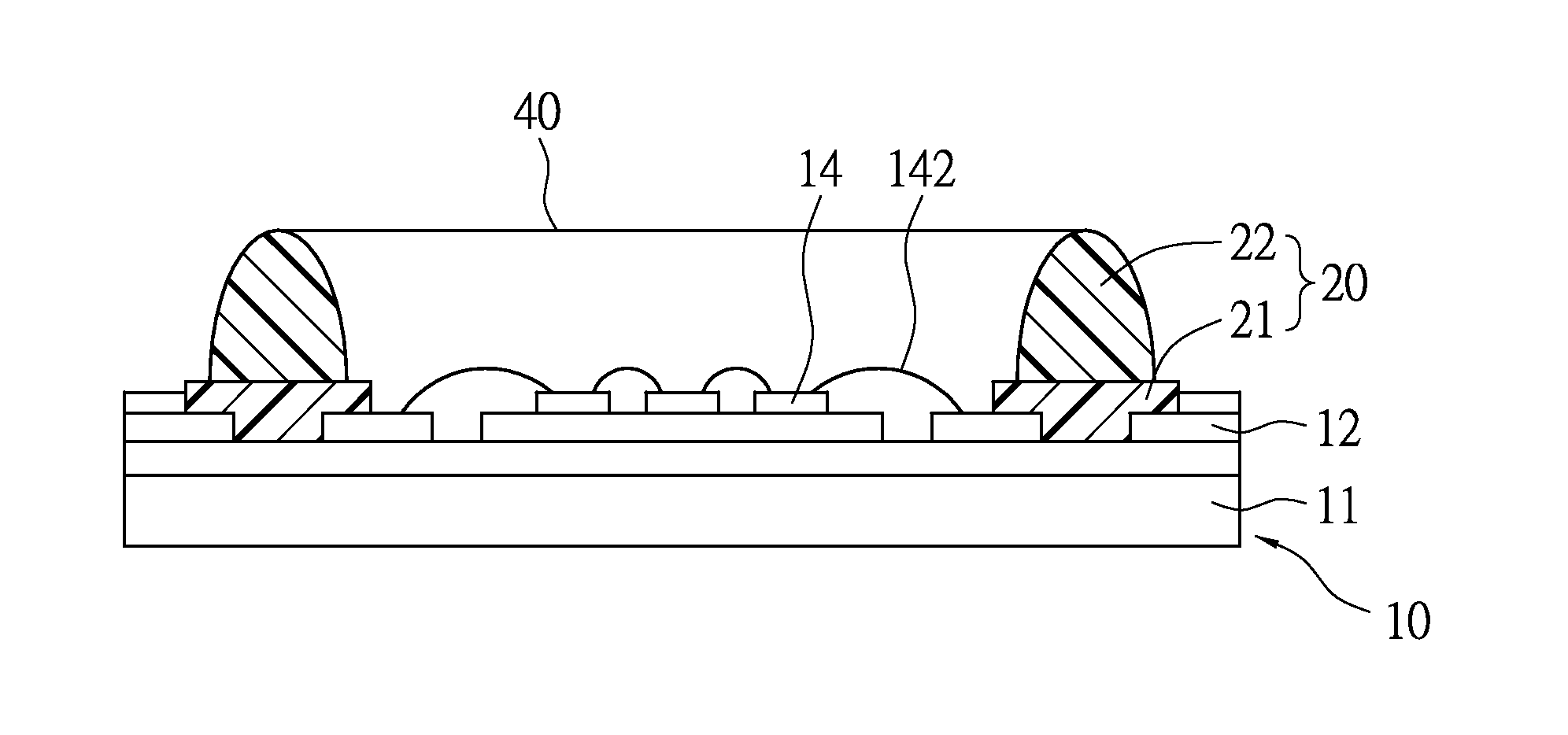
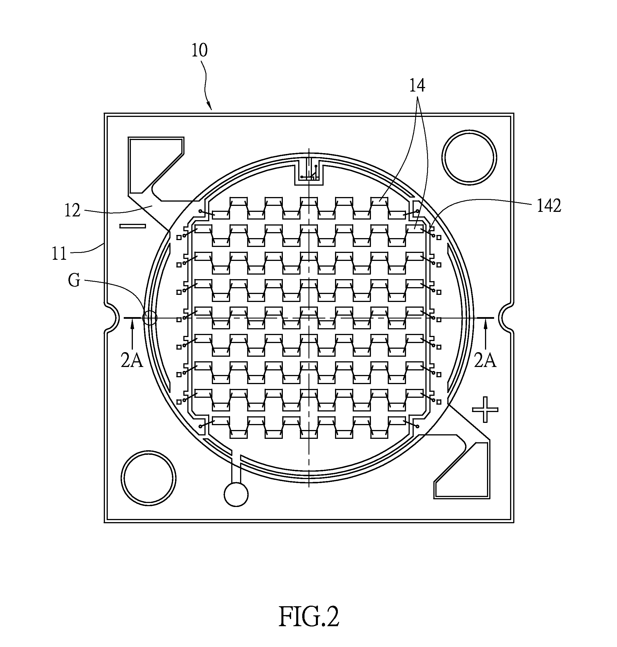
[0027]FIG. 2 shows a plan view of an LED package structure of the present disclosure. The LED package structure of the present disclosure includes a carrier 10 and a plurality of LED chips 14 disposed on the carrier 10. The LED chips 14 are connected to each other by wires. After the connection of LED chips 14, the LED chips 14 are further connected to a conductive layer 12 by wires (such as gold wires, metal alloy wires, etc.). An enlarged cross-sectional view of the LED package structure is shown in FIG. 2. FIG. 2A and FIG. 2B are schematic diagrams of the first glue-layer and the second glue-layer of the LED package structure of the present disclosure respectively. The method of manufacturing dam structure of LED package structure of the present disclosure includes the following steps. In first, as shown in FIG. 2A, a carrier 10 is provided. The carrier 10 has a flat top surface for at least one LED chip to be mounted thereon. The carrier 10 includes a substrate 11 and a conducti...

second embodiment

[0036]FIG. 3B shows a flowchart of a manufacturing method of an LED package structure of the present disclosure. In step S60, a carrier is provided. In step S8, the dam structure with bi-layer form is disposed on the carrier. In step S79, the dam structure with bi-layer is cured. After the dam structure is cured at step S79, step S61 is carried out. In step S61, at least one LED chip is disposed within the dam structure. Finally, the encapsulation process is carried out. As shown in step S62, an encapsulation resin is disposed within the dam structure for encapsulating the LED.

[0037]Regarding the relationship between the two sets of first and second parameters, according to one of the embodiments of the present disclosure, the first height setting L1-H and the first pressure setting L1-P for disposing the first glue-layer are lower than the second height setting L2-H and the second pressure setting L2-P for disposing the second glue-layer. In other words, a smaller height (i.e., the...


PUM


Abstract

An LED package structure includes a carrier mounted with a plurality of LED chips, a first glue-layer, a second glue-layer and an encapsulation resin filled within the first and the second glue-layers. The first glue-layer is formed on a top surface of the carrier and has a thin-film structure which is substantially flat on a top surface thereof. The second glue-layer is stacked on the first glue-layer. The second glue-layer has a height higher than that of the first glue-layer. The second glue-layer has a volume greater than that of the first glue-layer. The present invention also provides a method of LED package structure to stably produce a dam structure with uniform shape and high ratio of height / width.

Description

BACKGROUND OF THE INVENTION[0001]1. Field of the Invention[0002]The present invention relates to an LED package structure, a dam structure thereof, and a method of manufacturing the LED package structure thereof; in particular, to an LED package structure which has multiple LED chips disposed on the top surface of the carrier and a dam structure for enclosing a resin encapsulating the LED, and to a method of manufacturing the LED package structure thereof.[0003]2. Description of Related Art[0004]With advancement of LED package technology, integrated circuit and heat-dissipation techniques, the LED application is becoming ever more diverse.[0005]FIG. 1 shows a conventional LED package structure that includes a carrier 9, multiple LED chips 92 disposed on a top surface of the carrier 9, and a dam structure 94 enclosing the LED chips 92. The carrier 9 includes a conducting substrate 90, a dielectric layer D and a conductive layer 91. The LED chips 92 are connected to two sides of the c...

Claims


Application Information

Patent Timeline
IPC IPC(8): H01L33/48H01L33/52
CPCH01L25/0753H01L33/486H01L33/54H01L2933/0033H01L2933/005H01L2224/48091H01L2224/48137H01L2224/45144H01L33/52H01L2924/00014H01L2924/00
Inventor CHIU, KUO-MING
Owner LITE ON ELECTRONICS (GUANGZHOU) LTD
Learn More