Image sensor and method for fabricating the same
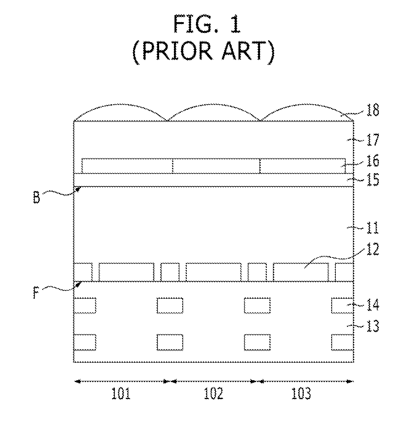
a technology of image sensor and fabrication method, which is applied in the field of image sensor, can solve the problems of reducing the photosensitivity and quantum efficiency of the image sensor, reducing the quantum efficiency (qe), and reducing the optical crosstalk characteristic (x-talk) characteristic, so as to prevent optical crosstalk and increase quantum efficiency
- Summary
- Abstract
- Description
- Claims
- Application Information
AI Technical Summary
Benefits of technology
Problems solved by technology
Method used
Image
Examples
first embodiment
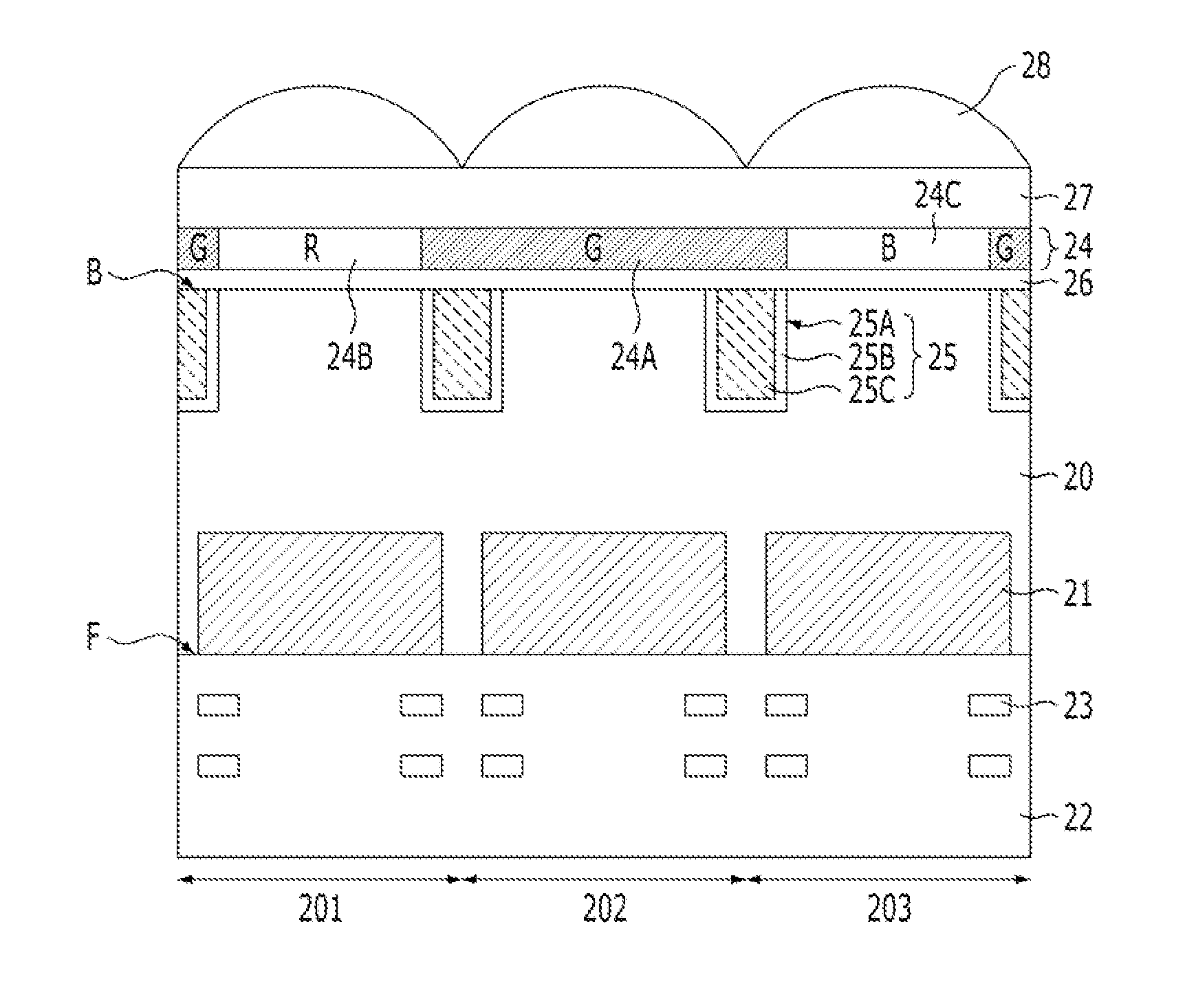
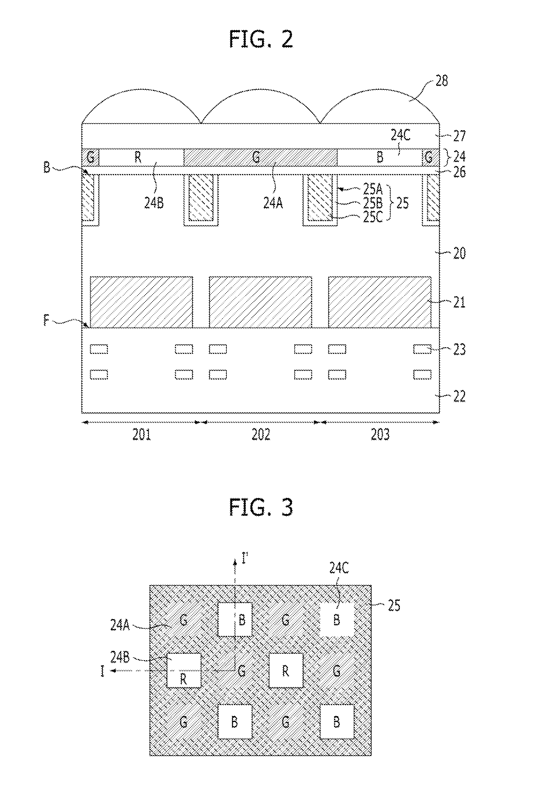
[0025]FIG. 2 is a cross-sectional view of an image sensor in accordance with the present invention.
[0026]Referring to FIG. 2, an image sensor in accordance with the first embodiment of the present invention may include a substrate 20, a light receiving element 21, an interlayer dielectric layer 22, a color filter 24, a light absorption unit 25, an anti-reflection layer 26, a planarized layer 27, and a micro lens 28. The substrate 20 has a plurality of unit pixel regions 201, 202, and 203. The light receiving element 21 is formed in each of the unit pixel regions 201, 202, and 203 of the substrate 20. The interlayer dielectric layer 22 is formed on a frontside F of the substrate 20 and includes a signal generation circuit 23. The color filter 24 is formed over a backside B of the substrate 20, corresponding to the opposite side of the frontside F. The light absorption unit 25 is formed in the backside B of the substrate 20, under the color filter 24. The anti-reflection layer 26 is f...
second embodiment
[0062]FIG. 6 is a cross-sectional view of an image sensor in accordance with the present invention.
[0063]Referring to FIG. 6, an image sensor in accordance with the second embodiment of the present invention may include a substrate 60, a light receiving element 61, an interlayer dielectric layer 62, a color filter 64, a light absorption unit 65, an anti-reflection layer 66, a planarized layer 67, and a micro lens 68. The substrate 60 has a plurality of unit pixel regions 601, 602, and 603. The light receiving element 61 is formed in each of the unit pixel regions 601, 602, and 603 of the substrate. The interlayer dielectric layer 62 is formed on a frontside F of the substrate 60 and includes a signal generation circuit 63. The color filter 64 is formed over a backside B of the substrate 60, corresponding to the opposite side of the frontside F. The light absorption unit 65 is formed between unit pixels in the backside B of the substrate 60 under the color filter 64. The anti-reflect...
third embodiment
[0081]FIG. 7 is a cross-sectional view of an image sensor in accordance with the present invention.
[0082]Referring to FIG. 7, an image sensor in accordance with the third embodiment of the present invention may include a substrate 70, a light receiving element 71, an interlayer dielectric layer 72, a color filter 74, a light absorption unit 75, an anti-reflection layer 76, a planarized layer 77, and a micro lens 78. The substrate 70 has a plurality of unit pixel regions 701, 702, and 703. The light receiving element 71 is formed in each of the unit pixel regions 701, 702, and 703 of the substrate 70. The interlayer dielectric layer 72 is formed on a frontside F of the substrate 70 and includes a signal generation circuit 73. The color filter 74 is formed over a backside B of the substrate 70, corresponding to the opposite side of the frontside F. The light absorption unit 65 is formed in the backside B of the substrate 70, corresponding to the opposite side of the frontside F. The a...
PUM
 Abstract
Description
Claims
Application Information
 - R&D
- Intellectual Property
- Life Sciences
- Materials
- Tech Scout
- Unparalleled Data Quality
- Higher Quality Content
- 60% Fewer Hallucinations
Browse by: Latest US Patents, China's latest patents, Technical Efficacy Thesaurus, Application Domain, Technology Topic, Popular Technical Reports.
© 2025 PatSnap. All rights reserved.Legal|Privacy policy|Modern Slavery Act Transparency Statement|Sitemap|About US| Contact US: help@patsnap.com


