Eureka AIR delivers breakthrough ideas for toughest innovation challenges, trusted by R&D personnel around the world.

Methods for fabricating bulk heterojunctions using solution processing techniques

a heterojunction and solution processing technology, applied in the field of heterojunction materials, can solve the problems of limited exciton diffusion length of plastic photovoltaic devices, incompatibility of traditional silicon based material processing techniques with plastic substrates,

Inactive Publication Date: 2014-05-29
ARIZONA STATE UNIVERSITY
View PDF7 Cites 51 Cited by
  • Summary
  • Abstract
  • Description
  • Claims
  • Application Information

AI Technical Summary

Benefits of technology

The present invention describes methods for fabricating heterojunction materials using solution processing techniques. The methods involve contacting a donor material and an acceptor material with a solvent system that comprises at least two individual solvents, wherein the solvents have different boiling points. The solvent system can also contain a halogenated compound or dichlorobenzene. The methods can dissolve at least a portion of both donor and acceptor materials. The invention also provides devices that comprise heterojunction materials made from the various methods. The technical effects include improved efficiency and performance of organic light emitting devices and photovoltaic devices.

Problems solved by technology

Techniques utilized for processing traditional silicon based materials are not compatible with plastic substrates due to, for example, temperature limitations.
Similarly, plastic photovoltaic devices suffer from limited exciton diffusion lengths, such that only excitons near the p-n interface can be collected.

Method used


Image

  • Methods for fabricating bulk heterojunctions using solution processing techniques
  • Methods for fabricating bulk heterojunctions using solution processing techniques
  • Methods for fabricating bulk heterojunctions using solution processing techniques

Examples


example 1

Preparation of Inventive P3HT / PCBM Blend

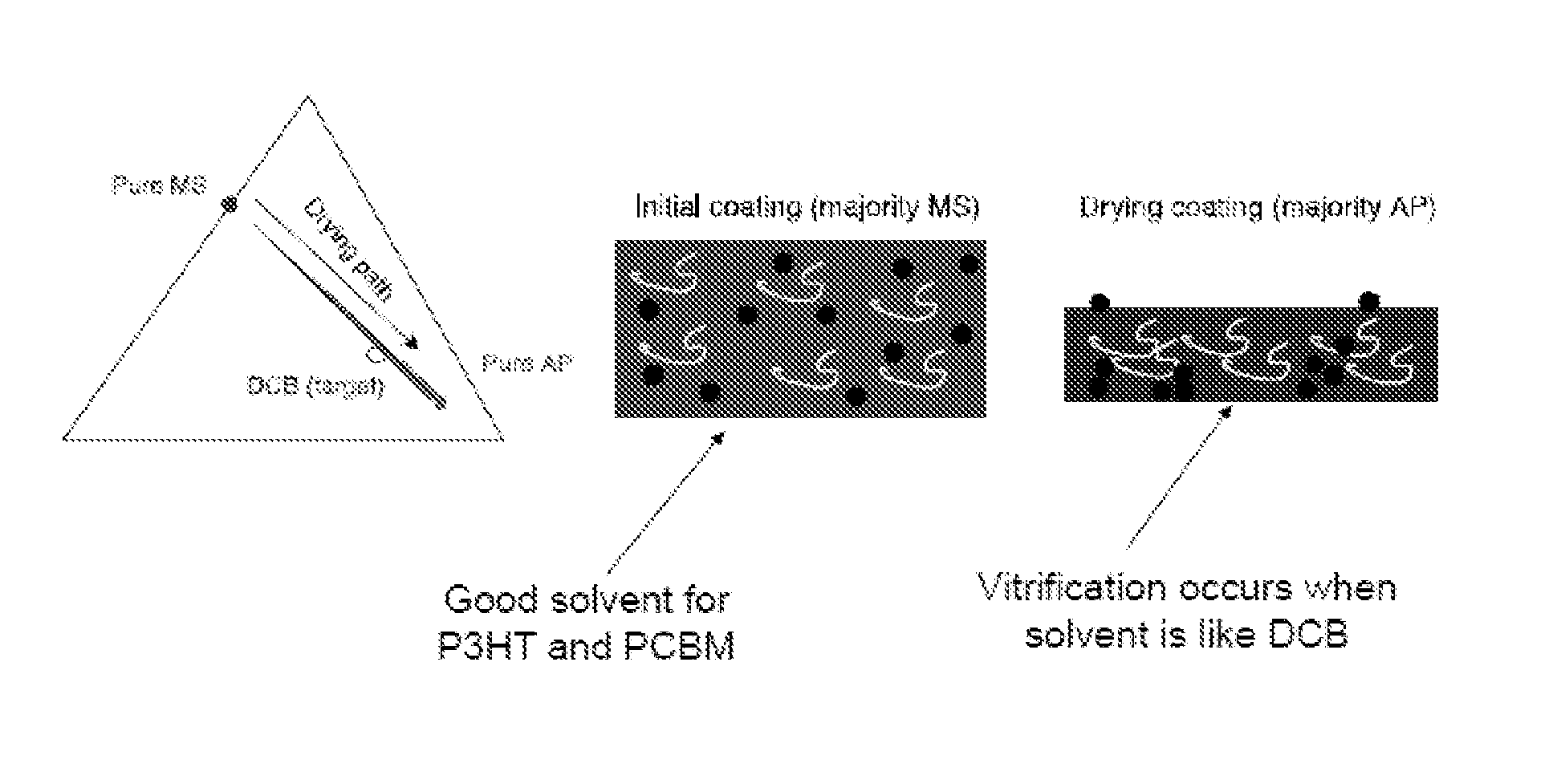
[0068]In a first example, a P3HT / PCBM blend was prepared. Regioregular P3HT (Rieke Metals, 4002E) and PCBM (Solenne) were dissolved in a 1:1 ratio to 1.0 wt % in either MS (98%, Alfa-Aesar) or a 80 vol. % MS-20 vol. % AP (Sigma-Aldrich) solvent mixture by heating and stirring for 2 h at 75° C. The mixture was then cooled slowly to ambient temperature.

example 2

Preparation of Comparative P3HT / PCBM Blend

[0069]In a second example, a comparative P3HT:PCBM blend (1.5 wt %, 1:1 weight ratio) was prepared by dissolving in DCB (Sigma-Aldrich) and stirring for 24 h at 40° C. The resulting mixture was then cooled slowly to ambient temperature.

example 3

Preparation of Solar Cells

[0070]In a third example, BHJ solar cells having the structure ITO / PEDOT / P3HT:PCBM / BCP / Al were fabricated by spin-coating the blends of P3HT:PCBM solutions prepared in Examples 1 and 2. Before the fabrication of the devices, the ITO-coated glass substrates were cleaned by scrubbing with detergent and then subjected to ultrasonic treatment sequentially in deionized water, acetone and isopropyl alcohol. The cleaned substrates were then UV-ozone treated for 40 min to remove residual organic contaminants. The cleaned ITO-coated glass substrates were modified by spin-coating a thin layer (˜40 nm) of PEDOT:PSS (Baytron P, Bayer) and cured at 200° C. for 30 min. The active layers were spin-coated in a nitrogen-filled glove box. The spin-coating conditions were optimized for each solution by adjusting the spin-coating speed and time in order to obtain the similar film thickness and drying time for the as-cast films. The as-cast films were dried overnight. After dry...


PUM


Abstract

Solvent mixtures useful for processing bulk heterojunction materials and methods for selecting the same are disclosed, wherein Hansen solubility parameters are utilized to select the solvent mixture. A solvent system using a fully nonhalogenated solvent mixture is disclosed. Also disclosed is a solvent mixture containing 20 vol. % acetophenone (AP) in mesitylene (MS), wherein the performance of the solvent system is comparable to dichlorobenzene.

Description

BACKGROUND[0001]1. Technical Field[0002]The present disclosure relates to heterojunction materials, and specifically to methods for fabricating a heterojunction using solution processing techniques.[0003]2. Technical Background[0004]Semiconductor materials and heterojunction composites thereof are of significant interest for use in light absorbing and light emitting devices. Traditional organic solar cell devices can contain multiple layers, for example, an anode, a donor-type material, an acceptor-type material, an exciton blocking material, and a cathode. In recent years, significant research has been employed in the processing of semiconductor materials for such applications, but further developments are needed to facilitate the use of these materials in electronic devices.[0005]Techniques utilized for processing traditional silicon based materials are not compatible with plastic substrates due to, for example, temperature limitations. Similarly, plastic photovoltaic devices suff...

Claims


Application Information

Patent Timeline
Patent Type & Authority Applications(United States)
IPC IPC(8): H01L21/02
CPCH10K71/15H10K71/40H10K10/468H10K30/30H10K30/50H01L21/02628
Inventor VOGT, BRYAN D.LI, JIANPARK, CHOONG-DO
Owner ARIZONA STATE UNIVERSITY
Why Eureka
Eureka Blog
Learn More