Method for growing epitaxial diamond
a technology of epitaxial diamond and diamond, which is applied in the direction of single crystal growth, polycrystalline material growth, chemistry apparatus and processes, etc., can solve the problems of deformation and cracks releasing stress, cracks, and problems that remain to be solved, and achieve the effect of desired thickness and good quality
- Summary
- Abstract
- Description
- Claims
- Application Information
AI Technical Summary
Benefits of technology
Problems solved by technology
Method used
Image
Examples
embodiment i
The Embodiment I
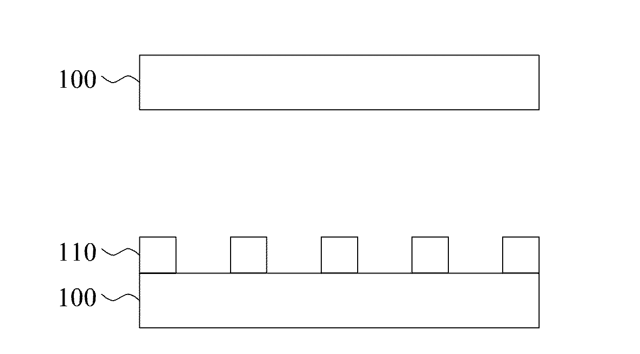
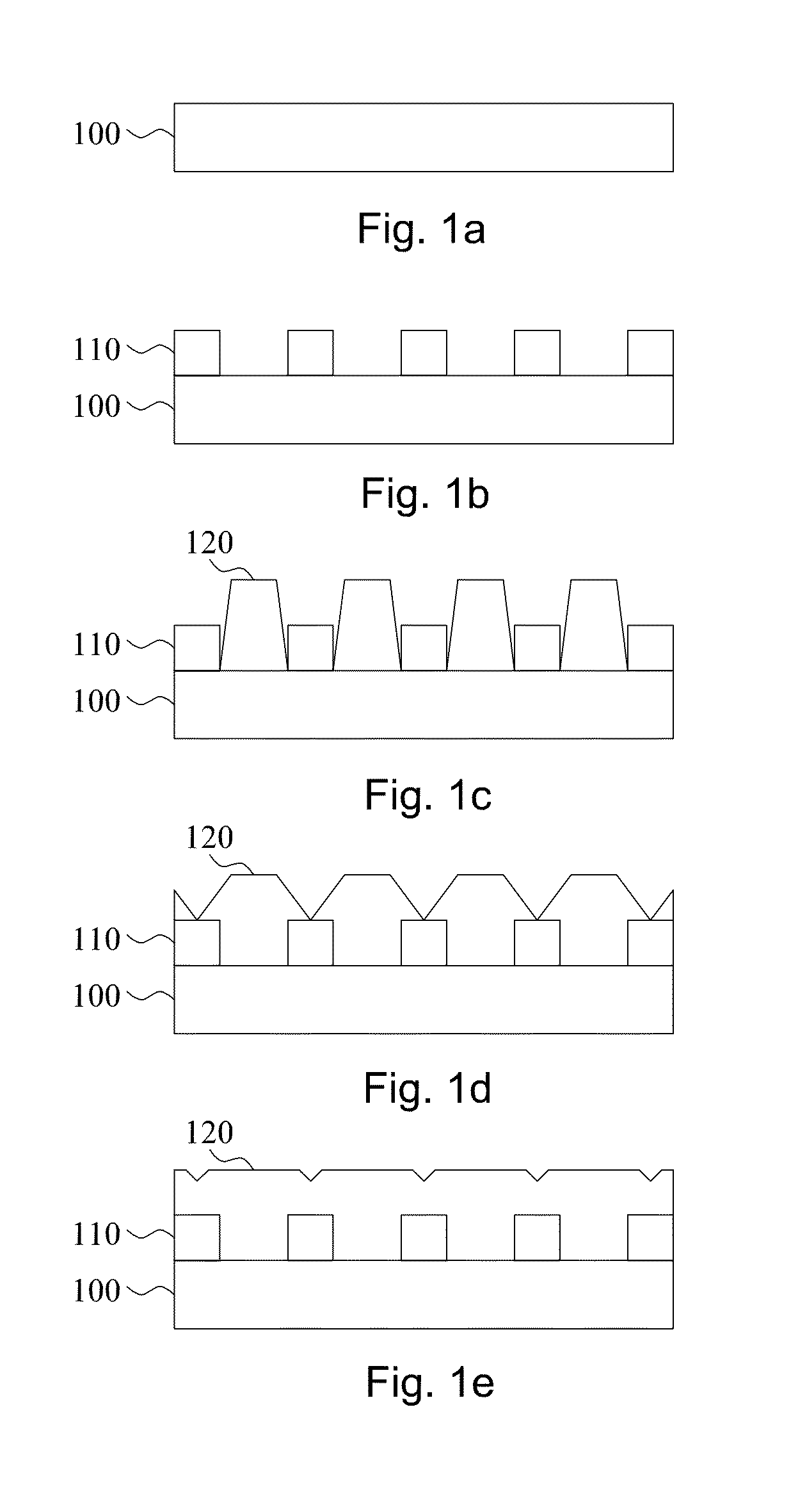
[0027]A (111) single crystal diamond manufactured by HPHT (high pressure and high temperature) process is adopted as a diamond substrate and is followed by a nickel layer with thickness of 20 nm deposited on the diamond substrate via electron beam evaporation method. Lattice mismatch between nickel and diamond is 1.4%; dissolution rate of carbon in nickel is 0.9 wt % (>1000° C.). There is no C—Ni reactant according to the C—Ni phase diagram. Subsequently, the substrate is placed into a microwave plasma chemical deposition system for annealing processes at high temperature. The process parameters are: microwave power 800 W, pressure 80 torr, pure hydrogen, deposition time 10 min, substrate temperature 850° C.-1100° C. After the annealing process, a (111) epitaxial diamond film is deposited on the metallic layer and the diamond substrate. Growth parameters of the epitaxial diamond film are that: microwave power 800 W, pressure 80 torr, ratio of hydrogen and methane is ...
embodiment ii
The Embodiment II
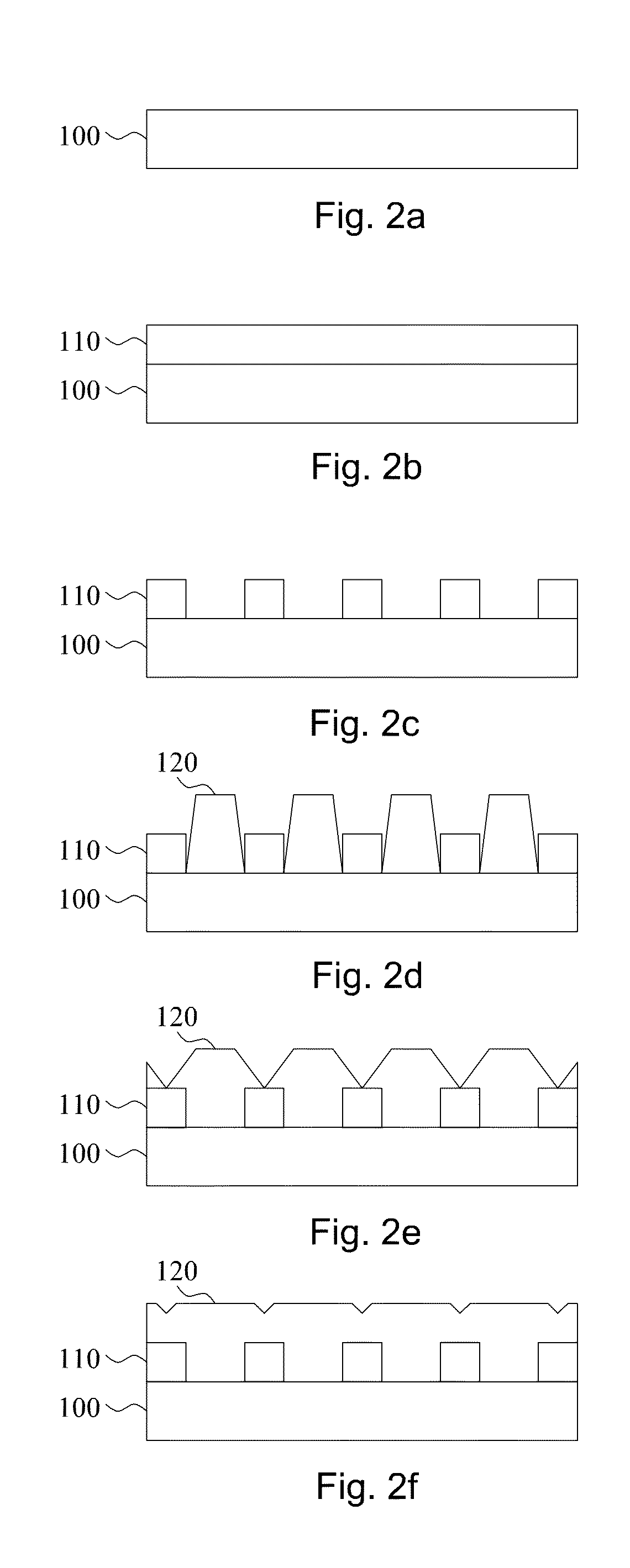
[0028]A (100) single crystal diamond manufactured by HPHT (high pressure and high temperature) process is adopted as a diamond substrate and is followed by a nickel layer with thickness of 20 nm deposited on the diamond substrate via electron beam evaporation method. Lattice mismatch between nickel and diamond is 1.4%; dissolution rate of carbon in nickel is 0.9 wt % (>1000° C.). There is no C—Ni reactant according to the C—Ni phase diagram. Subsequently, the substrate is placed into a microwave plasma chemical deposition system for an annealing process at high temperature. The process parameters are: microwave power 800 W, pressure 80 torr, pure hydrogen, deposition time 10 min, substrate temperature 850° C.-1100° C. After the annealing process, a (100) epitaxial diamond film is deposited on the metallic layer and the diamond substrate. Growth parameters of the epitaxial diamond film are as follow: microwave power 800 W, pressure 80 torr, ratio of hydrogen and meth...
PUM
| Property | Measurement | Unit |
|---|---|---|
| thickness | aaaaa | aaaaa |
| thickness | aaaaa | aaaaa |
| thickness | aaaaa | aaaaa |
Abstract
Description
Claims
Application Information
 - R&D
- Intellectual Property
- Life Sciences
- Materials
- Tech Scout
- Unparalleled Data Quality
- Higher Quality Content
- 60% Fewer Hallucinations
Browse by: Latest US Patents, China's latest patents, Technical Efficacy Thesaurus, Application Domain, Technology Topic, Popular Technical Reports.
© 2025 PatSnap. All rights reserved.Legal|Privacy policy|Modern Slavery Act Transparency Statement|Sitemap|About US| Contact US: help@patsnap.com


