Method for manufacturing printed circuit board

Active Publication Date: 2014-02-27
AVARY HLDG (SHENZHEN) CO LTD +1
View PDF17 Cites 8 Cited by
  • Summary
  • Abstract
  • Description
  • Claims
  • Application Information

AI Technical Summary

Benefits of technology

The patent text describes a problem where burrs (small metal pieces) are formed when punching a PCB sheet. These burrs can damage the contact pad on the PCB unit, leading to poor performance. To prevent this, a high-energy laser cutting method is used, but this may cause the contact pad to oxidize due to the close proximity of the laser beam to the edge of the PCB sheet. The technical effect of this patent text is to provide a solution to prevent burr formation and oxidation of the contact pad while still maintaining a high-quality PCB unit.

Problems solved by technology

When a nearest distance between a contact pad on the PCB unit and an edge of the PCB unit is less than 4 millimeters, the burrs may drop on the contact pad, resulting in a bad performance of the contact pad.
However, the surface of the contact pad may be oxidized by the high-energy laser beam because of the small nearest distance between the contact pad and the edge of the PCB sheet.

Method used


Image

  • Method for manufacturing printed circuit board
  • Method for manufacturing printed circuit board
  • Method for manufacturing printed circuit board

Examples


first embodiment

[0019]A method for manufacturing a PCB includes the following steps.

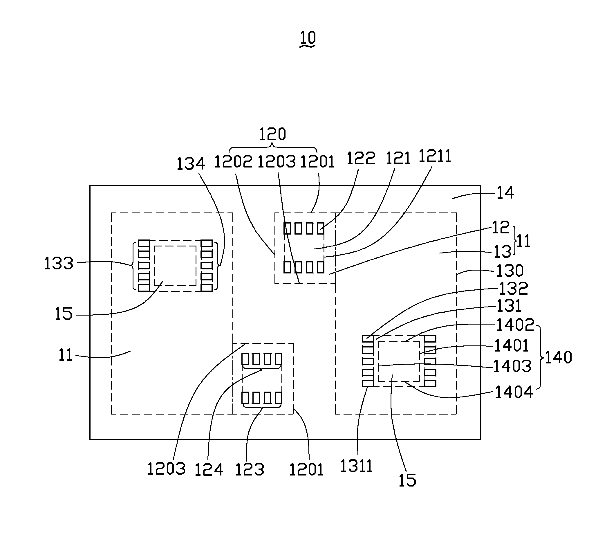
[0020]FIG. 1 shows that, in step (1), a PCB sheet 10 is provided.

[0021]In this embodiment, the PCB sheet 10 is rectangular. The PCB sheet 10 includes two PCB units 11, a first unwanted portion 14 and two second unwanted portions 15. The two PCB units 11 are surrounded by the first unwanted portion 14. The second unwanted portions 15 are defined in the PCB units 11.

[0022]In this embodiment, the PCB sheet 10 can be formed by a plurality of processes comprising a drilling process, a electrochemical deposition process, a photolithography process and an etching process.

[0023]The PCB unit 11 includes a first product portion 12 and a second product portion 13 connected to the first product portion 12.

[0024]The first product portion 12 is also rectangular. A first imaginary boundary line 120 is defined between the first product portion 12 and the first unwanted portion 14. The first imaginary boundary line 120 includes a f...

second embodiment

[0043]A method for manufacturing a printed circuit board includes the following steps.

[0044]Step 1 of this embodiment is same as step (1) of the first embodiment.

[0045]FIG. 6 shows that, in step 2, the PCB sheet 10 is punched along the first imaginary boundary line 120 and the third imaginary boundary lines 140, thereby forming a plurality of first through slots 9101 along the first imaginary boundary lines 120, and two hollow portions 9102 are surrounded by the two third imaginary boundary lines 140. The first through slots 9101 are separated by a plurality of first interconnect links 9106 interconnecting the first unwanted portion 14 and the first product portion 12. A plurality of first burrs 9103 are generated on an inner surface of the first through slots 9101, and a plurality of second burrs 9105 are generated on an inner surface of the hollow portions 9102 during the punching process.

[0046]That is to say, the printed circuit board sheet 10 is punched along a section of the i...


PUM

PropertyMeasurementUnit
Lengthaaaaaaaaaa
Poweraaaaaaaaaa
Poweraaaaaaaaaa

Abstract

A method for manufacturing a PCB includes certain steps. A printed circuit board sheet is provided. The printed circuit board includes an unwanted portion and a printed circuit board unit which includes a plurality of contact pads. An imaginary boundary line is defined between the printed circuit board unit and the unwanted portion. Each of the contact pads defines an outline. A nearest distance between the outline and the imaginary boundary line is less than 4 millimeters. The printed circuit board sheet is punched along the imaginary boundary line, forming one hollow portion or a plurality of through slots. A plurality of burrs is generated on an inner surface of the hollow portion or the through slots. The burrs are removed using a low-energy laser cutting process, thereby obtaining a printed circuit board. A laser power used in the low-energy laser cutting process is 5-8 watts.

Description

BACKGROUND[0001]1. Technical Field[0002]The present disclosure relates to printed circuit boards, particularly to a method for manufacturing a printed circuit board.[0003]2. Description of Related Art[0004]Usually, a method for manufacturing a printed circuit board (PCB) includes the following processes. First, a PCB sheet including a PCB unit and an unwanted portion is provided. A plurality of contact pads is formed on the PCB unit. Imaginary boundary lines are defined between the PCB unit and the unwanted portion. Second, the PCB sheet is punched along the imaginary boundary lines. Thus, a plurality of through slots is forming between the PCB unit and the unwanted portion, and a plurality of interconnect links interconnect the PCB unit and the unwanted portion and separating the adjacent through slots. Third, a plurality of components is mounted on the contact pads of the PCB unit. Finally, the PCB unit is separated from the unwanted portion by punching the interconnect links, the...

Claims


Application Information

Patent Timeline
IPC IPC(8): H05K3/00
CPCH05K3/005H05K3/0032H05K3/0052H05K2201/09063H05K2203/0346H05K2203/107Y10T29/49124
Inventor LIU, RUI-WULEE, YU-HSIENYU, WEN-HSIN
Owner AVARY HLDG (SHENZHEN) CO LTD
Why Eureka
Try Eureka