Power supply control circuit and signal processing circuit
- Summary
- Abstract
- Description
- Claims
- Application Information
AI Technical Summary
Benefits of technology
Problems solved by technology
Method used
Image
Examples
embodiment 1
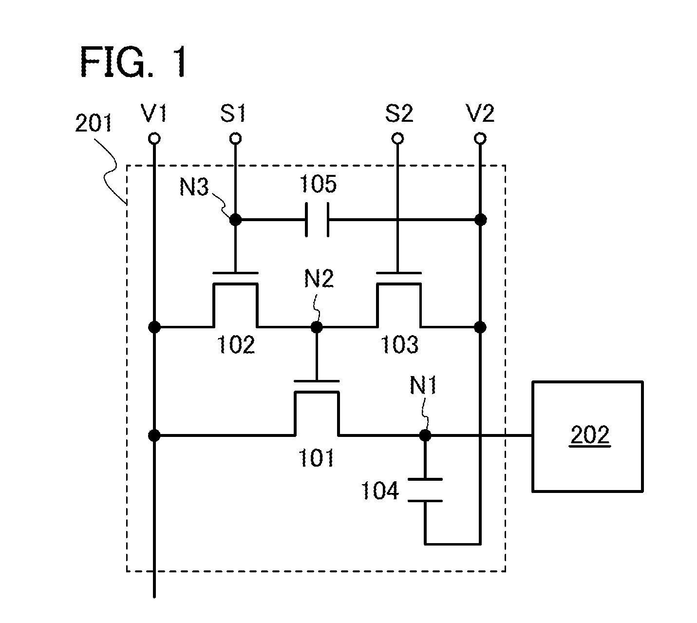
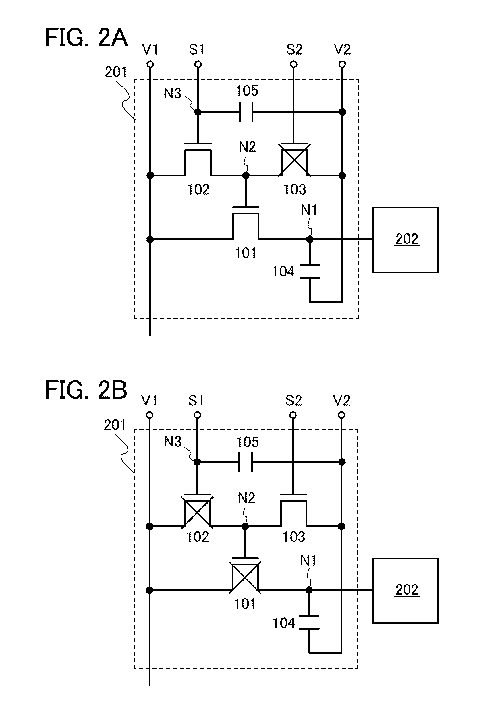
[0044]In this embodiment, an example of a signal processing circuit provided with a power supply control circuit is described with reference to FIG. 1 and FIGS. 2A and 2B.
[Configuration of Power Supply Control Circuit]
[0045]A power supply control circuit according to one embodiment of the present invention includes a first switching element for controlling power supply or stop of power supply, a switching control portion for controlling on or off of the first switching element, and a capacitor for holding the power supply potential when the first switching element is turned off. The switching control portion includes a second switching element and a third switching element.
[0046]A power supply control circuit 201 illustrated in FIG. 1 includes a transistor 101, a transistor 102, a transistor 103, a capacitor 104, and a capacitor 105. Further, a processor 202 includes one or a plurality of volatile memory devices such as a register or a cache memory.
[0047]One of a source and a drain ...
embodiment 2
[0064]In this embodiment, description is made, with reference to FIG. 3, FIGS. 4A and 4B, FIGS. 5A to 5D, and FIG. 6, on a method for driving a signal processing circuit 200 in the case where power supply is suddenly stopped after the power is supplied to the processor 202.
[0065]FIG. 3 illustrates a block diagram of the signal processing circuit 200 including the power supply control circuit 201. The signal processing circuit 200 includes the power supply control circuit 201, the processor 202, a detection circuit 203, a processor 204, and a non-volatile memory device 205. Here, the processor 202 is a main processor for controlling operation of electronic devices including the signal processing circuit 200. The processor 204 is a sub-processor that operates when power supply to the electronic devices is stopped. Further, the detection circuit 203, the processor 204, the memory device 205, and the processor 202 are connected to each other through wirings (e.g. a wiring L1).
[0066]The ...
embodiment 3
[0092]In this embodiment, a part of a cross section of the power supply control circuit that is described in the above embodiments will be described with reference to FIG. 6. FIG. 6 illustrates a structure in which the transistor 101 and the capacitor 104 which are included in the power supply control circuit 201 are stacked over transistors 510 and 520 which are included in the processor 202 shown in FIG. 3.
[0093]Note that description is made on the case where the transistor 101 and the transistor 510 are n-channel transistors and the transistor 520 is a p-channel transistor.
[0094]First, description is made on the transistor 510 and the transistor 520 which are formed in the lower portion.
[0095]An n-channel transistor 510 includes a channel formation region 501 provided in a substrate 500 including a semiconductor material, low-concentration impurity regions 502 and high-concentration impurity regions 503 (collectively simply referred to as impurity regions) with the channel format...
PUM
 Abstract
Description
Claims
Application Information
 - R&D
- Intellectual Property
- Life Sciences
- Materials
- Tech Scout
- Unparalleled Data Quality
- Higher Quality Content
- 60% Fewer Hallucinations
Browse by: Latest US Patents, China's latest patents, Technical Efficacy Thesaurus, Application Domain, Technology Topic, Popular Technical Reports.
© 2025 PatSnap. All rights reserved.Legal|Privacy policy|Modern Slavery Act Transparency Statement|Sitemap|About US| Contact US: help@patsnap.com


