
Analog-to-digital signal conversion method and apparatus therefor

a digital signal and conversion method technology, applied in analogue/digital conversion, physical parameter compensation/prevention, instruments, etc., can solve the problems of increasing fabrication time and manufacturing costs, and the area cannot be reduced, so as to increase reduce the variable capacitance value of the capacitor bank.

Inactive Publication Date: 2014-01-09
RES & BUSINESS FOUND SUNGKYUNKWAN UNIV +1
View PDF0 Cites 2 Cited by
  • Summary
  • Abstract
  • Description
  • Claims
  • Application Information

AI Technical Summary

Benefits of technology

The patent text describes a method for adjusting the delay time of a device called a delay cell. The method involves using a capacitor bank to control the delay time. When the delay time increases, the capacitance value of the capacitor bank is reduced. When the delay time decreases, the capacitance value of the capacitor bank is increased. The method also involves monitoring the second digital output signal to determine if the delay time has increased or decreased. The technical effect of this patent is to provide a reliable and adjustable method for controlling the delay time of a device.

Problems solved by technology

A related art analog PLL circuit has a problem in that it requires a divider operable at high speed, and since a width-length ratio of a metal-oxide semiconductor (MOS) may be limited depending on noise, accuracy, or the like, of a current source, the area thereof cannot be reduced.
Also, since a loop filter includes a passive resistor and a capacitor, it takes up a relatively large area, and in order to secure a desired analog signal level, a voltage-controller oscillator (VCO) buffer, a local oscillator (LO) buffer, an output buffer, or the like, is required in order to increase power consumption.
In addition, when a process is changed, all the blocks are required to be substantially re-designed due to the sensitivity to process characteristics of the analog PLL circuit, increasing a fabrication time and manufacturing costs.

Method used


Image

  • Analog-to-digital signal conversion method and apparatus therefor
  • Analog-to-digital signal conversion method and apparatus therefor
  • Analog-to-digital signal conversion method and apparatus therefor

Examples


Embodiment Construction

[0037]Hereinafter, embodiments of the present invention will be described in detail with reference to the accompanying drawings. The invention may, however, be embodied in many different forms and should not be construed as being limited to the embodiments set forth herein. Rather, these embodiments are provided so that this disclosure will be thorough and complete, and will fully convey the scope of the invention to those skilled in the art. In the drawings, the shapes and dimensions of elements may be exaggerated for clarity, and the same reference numerals will be used throughout to designate the same or like elements.

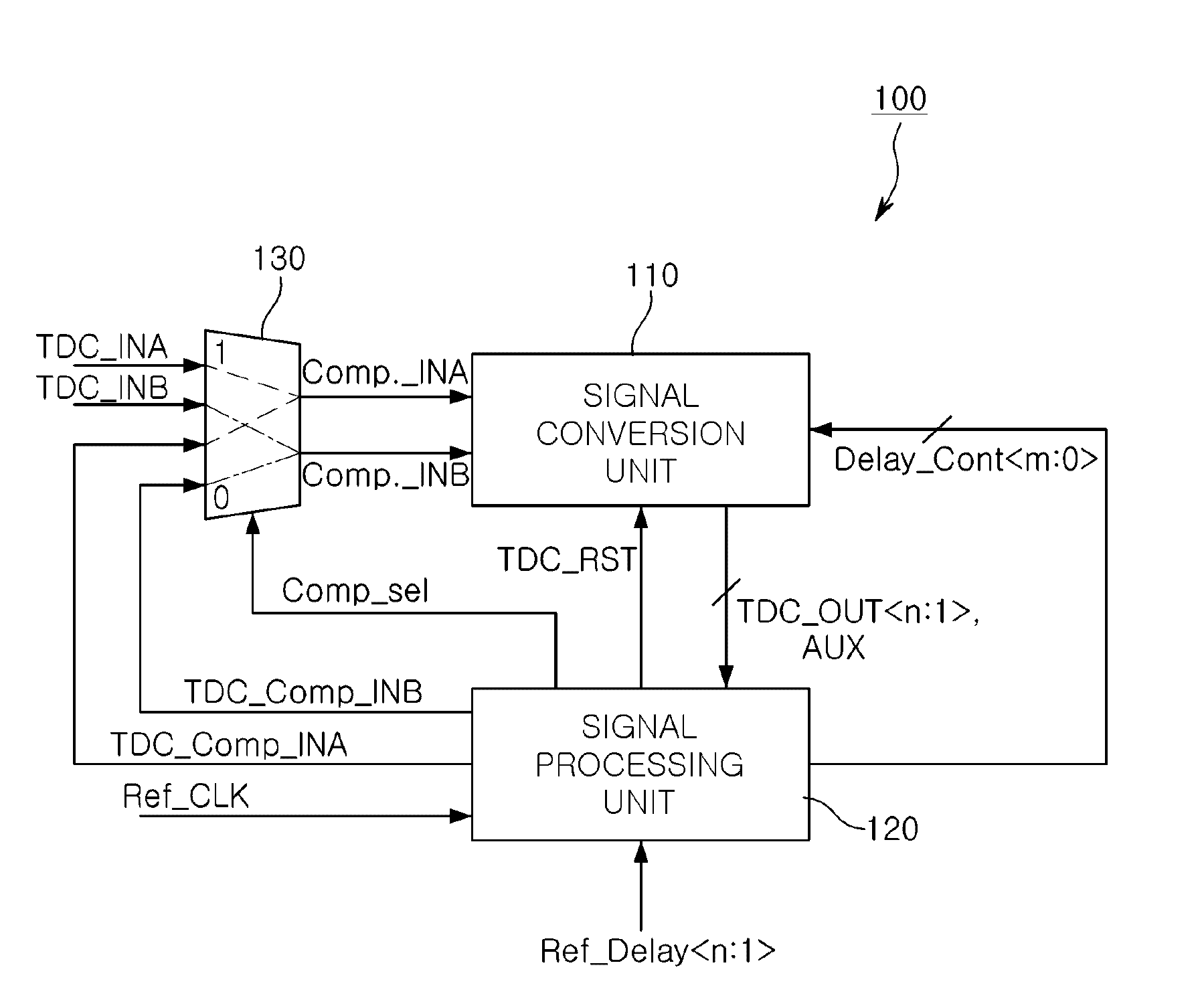
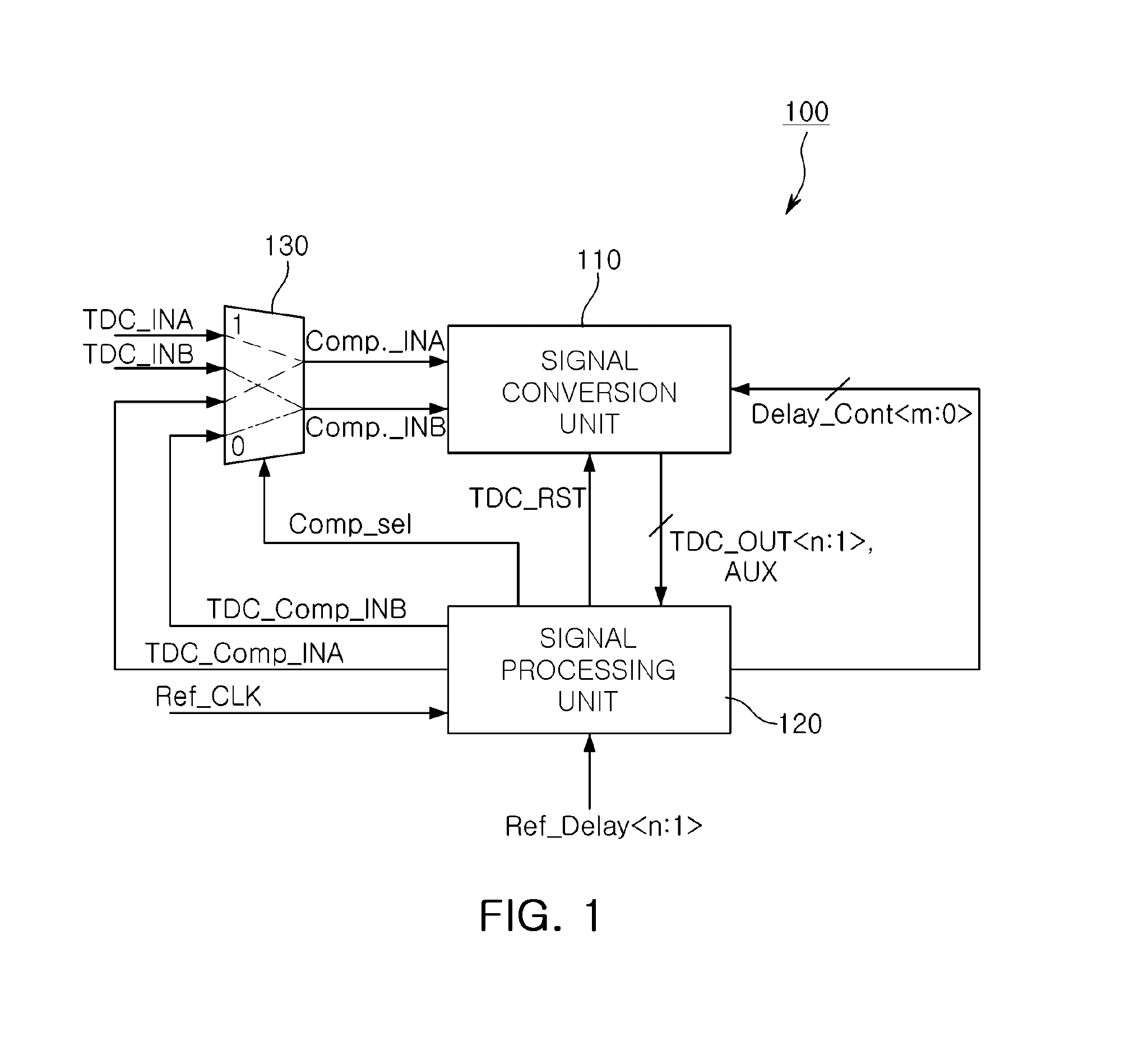
[0038]FIG. 1 is a block diagram of an analog-to-digital signal conversion apparatus according to an embodiment of the present invention.

[0039]Referring to FIG. 1, an analog-to-digital signal conversion apparatus 100 according to an embodiment of the present invention includes a signal conversion unit 110, a signal processing unit 120, and a signal selection unit 130...


PUM


Abstract

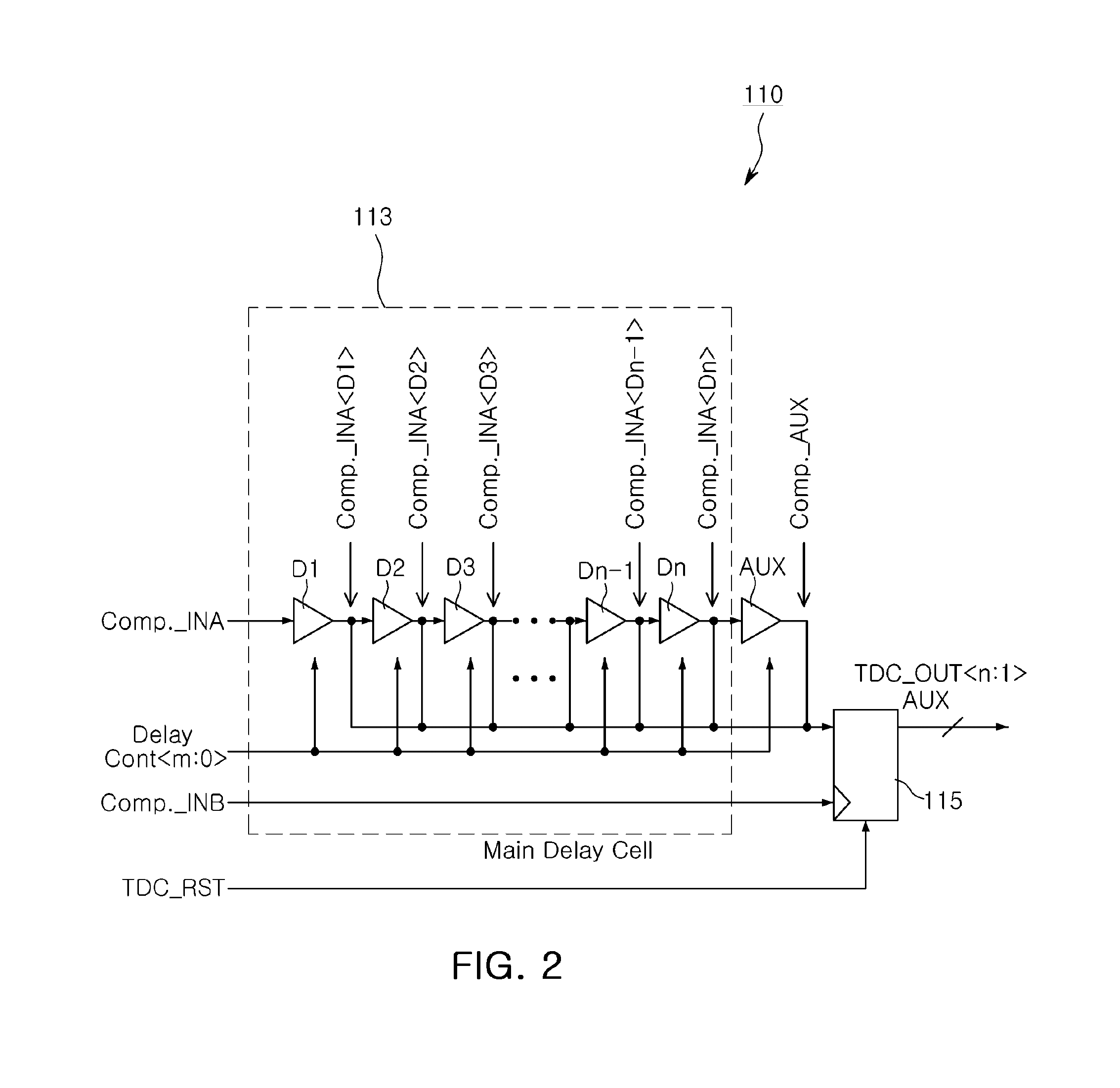
There are provided an analog-to-digital signal conversion method and apparatus therefor, and a digital phase locked loop circuit including the same. The analog-to-digital signal conversion method may include: generating a first digital output signal having N number of bits by comparing each of N number of delay signals detected from output terminals of N number of delay cells with a reference signal; generating a second digital output signal by comparing an auxiliary delay signal generated by an (N+1)th delay cell with the reference signal; and determining a change in a delay time of each of the N number of delay cells based on the first digital output signal and the second digital output signal.

Description

CROSS-REFERENCE TO RELATED APPLICATIONS[0001]This application claims the priority of Korean Patent Application No. 10-2012-0073053 filed on Jul. 4, 2012, in the Korean Intellectual Property Office, the disclosure of which is incorporated herein by reference.BACKGROUND OF THE INVENTION[0002]1. Field of the Invention[0003]The present invention relates to an analog-to-digital signal conversion method and apparatus therefor, and a digital phase locked loop circuit including the same.[0004]2. Description of the Related Art[0005]A phase locked loop (PLL) circuit is widely used to generate an application carrier frequency in a 4th-generation mobile communications system such as long term evolution (LTE), or the like, a cellular phone technology such as Bluetooth™, a global positioning system (GPS), a wideband code division multiple access (WCDMA) scheme, or the like, a wireless local area network (WLAN) such as an 802.11a / b / g scheme, or the like. A related art analog PLL circuit has a prob...

Claims


Application Information

Patent Timeline
Patent Type & Authority Applications(United States)
IPC IPC(8): H03M1/12H03M1/06
CPCH03M1/06H03M1/502
Inventor NA, YOO SAMLEE, KANG YOONPU, YOUNG GUNPARK, HYUNG GUKIM, HONG JINKIM, YOO HWANLEE, DONG SU
Owner RES & BUSINESS FOUND SUNGKYUNKWAN UNIV
Learn More