
Capacitor formed in insulated pores of an anodized metal layer

a technology of anodized metal and capacitor, applied in the direction of capacitor, semiconductor device details, semiconductor/solid-state device devices, etc., can solve the problems of low access resistance, degrade the performance of such components, and the storage requirement problem relating to the use of high-value capacitors arises. , to achieve the effect of low access resistan

Active Publication Date: 2019-12-03
COMMISSARIAT A LENERGIE ATOMIQUE ET AUX ENERGIES ALTERNATIVES +1
View PDF16 Cites 0 Cited by
  • Summary
  • Abstract
  • Description
  • Claims
  • Application Information

AI Technical Summary

Benefits of technology

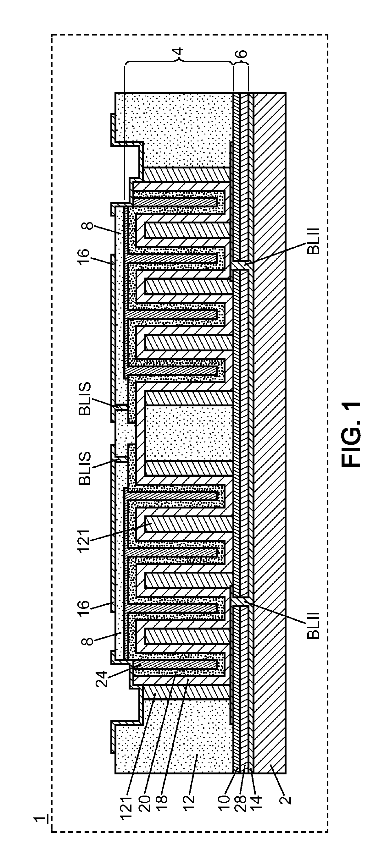
The invention is a capacitor structure that has a limited size, allowing for high integration. It uses a lower electrode and upper and lower insulation strips to stack several capacitors on top of each other, resulting in increased capacitance and improved integration. The structure has two capacitors in parallel, adding to the high value with a constant footprint.

Problems solved by technology

The integration of passive components and, more specifically, capacitors in integrated active or passive circuits is an important issue for developers.
In fact, during the integration of such components, technological compatibility problems arise between the processes for manufacturing capacitors, for example, and passive or active components.
In addition, storage requirement problems connected to the use of high-value capacitors arise.
However, such structures have relatively high internal resistance, which degrades the performance of such components and limits their integration in active circuits.
In addition, despite relatively high area ratios, thanks to the use of anodized layers, the densities of MIM capacitors thus obtained remain relatively low.
Consequently, during the design of high-value capacitors, space requirement problems associated with this type of technology arise.

Method used


Image

  • Capacitor formed in insulated pores of an anodized metal layer
  • Capacitor formed in insulated pores of an anodized metal layer
  • Capacitor formed in insulated pores of an anodized metal layer

Examples


Embodiment Construction

[0057]First, it should be noted that all figures illustrating the cross-sectional views of the capacitor structure as well as all figures illustrating the stacks of layers but also those representing the steps of the structure production process are not to scale. In addition, the different thicknesses are not realistically represented. For the sake of simplification, in the description and in the figures, elements that are common to all structures bear the same references.

[0058]The invention will be more specifically described in a non-limiting example of a Metal-Insulator-Metal type capacitor structure application that will subsequently be called in the rest of the description a MIM type capacitor structure. The MIM type capacitor structure example described below comprises a structured layer and more specifically a layer of nanostructured metal comprising a plurality of nanopores with a diameter d. The pores from the following description are nanopores but the invention can also b...


PUM


Abstract

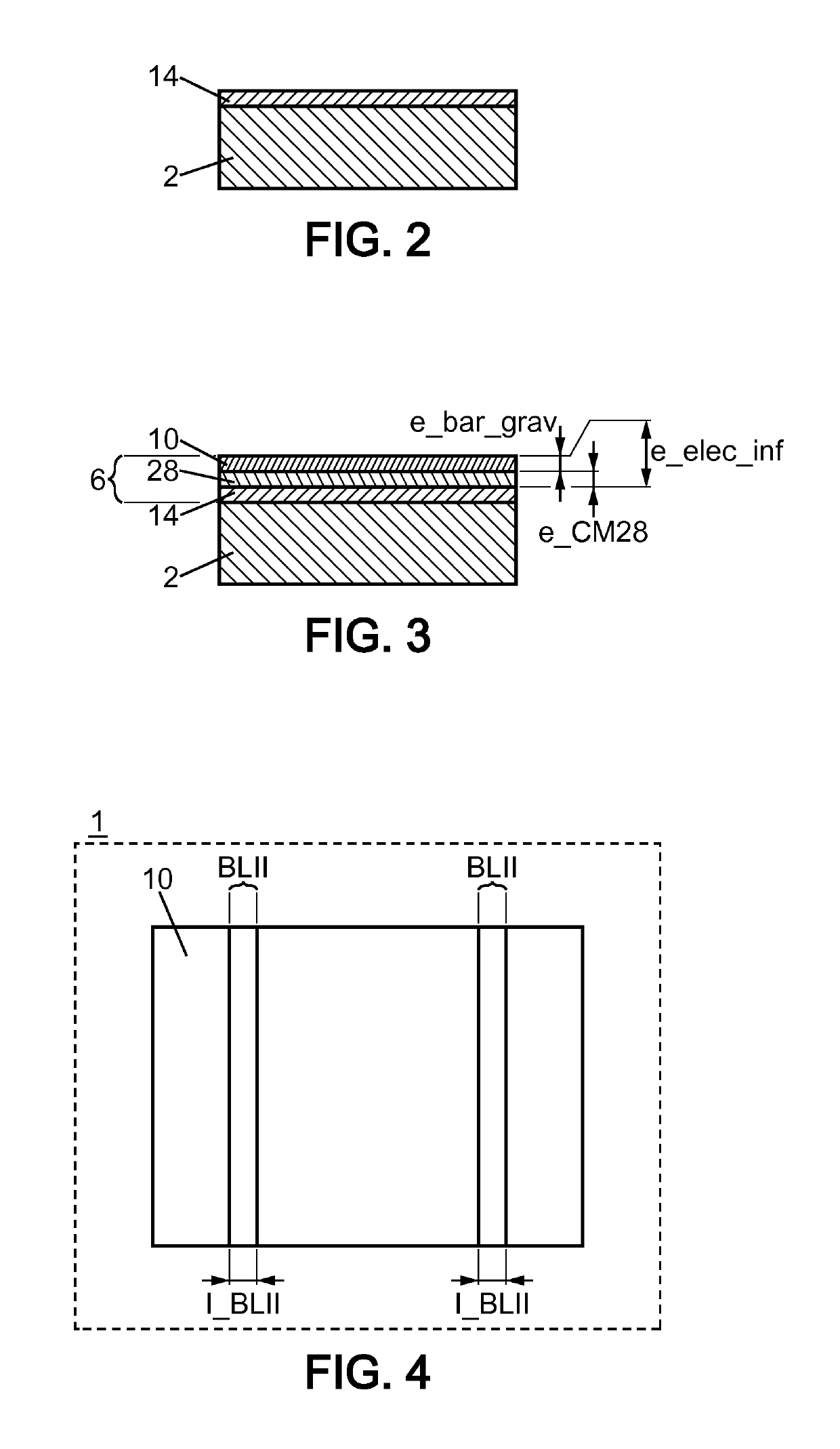
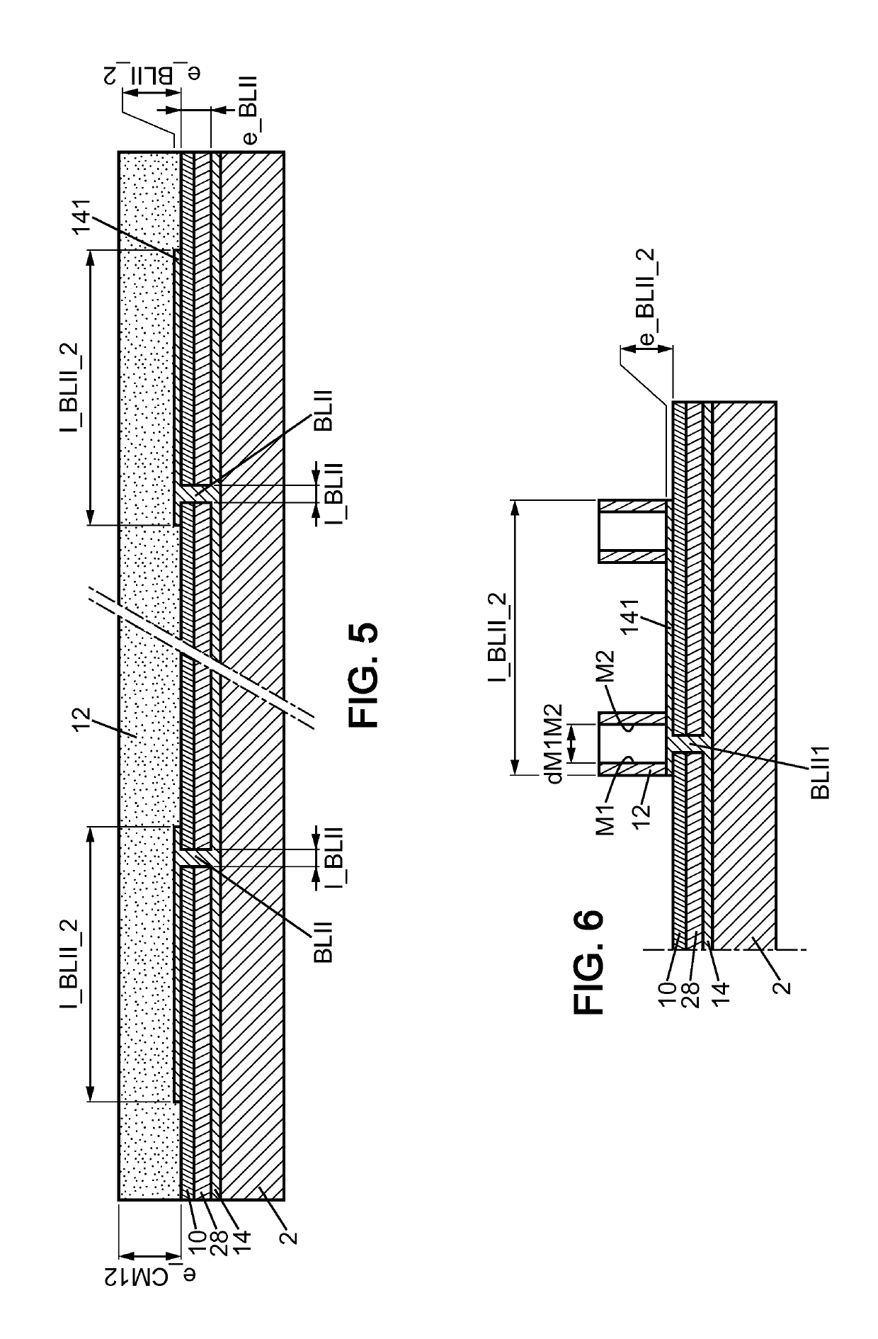
A Metal-Insulator-Metal type capacitor structure (1) comprising a substrate (2), a first electrically insulating layer (14) placed on the substrate (2), a lower electrode (6) placed on the first insulating layer (14), a layer of structured metal (12) comprising a plurality of pores disposed on the lower electrode (6), a MIM capacitor (4) comprising a first conductive layer (18) placed on the structured metal layer (12) in contact with the lower electrode (6) and inside the pores, a dielectric layer (20) covering the first conductive layer (18), a second conductive layer (24) covering the dielectric layer (20) in contact with an upper electrode (8) placed on the MIM capacitor (4) and a second electrically insulating layer (16) placed on the upper electrode (8).

Description

CROSS-REFERENCE TO RELATED APPLICATIONS[0001]This application is a National Stage entry of International Application No. PCT / FR2014 / 052754, filed on Oct. 29, 2014, which claims priority to French Application No. 1360555, filed on Oct. 29, 2013, the contents of each of these priority applications are hereby incorporated by reference in their entirety.TECHNICAL FIELD[0002]The present invention generally relates to Metal-Insulator-Metal capacitance. More specifically, the invention relates to a structure with a Metal-Insulator-Metal type capacitance from which a stack of Metal-Insulator-Metal type capacitors can be made.[0003]The invention finds applications, in particular, in the field of microelectronics and more specifically in the field of passive and / or active components used for example in medical devices, in energy management devices or else in avionics.BACKGROUND[0004]Thanks to technological developments in microelectronics, it is now possible to integrate several complex funct...

Claims


Application Information

Patent Timeline
IPC IPC(8): H01L27/08H01G4/005H01L21/3213H01L21/02H01L49/02
CPCH01L21/32133H01L21/02258H01L28/60H01L27/0805H01G4/005H01L23/5223H01L28/90H01L2924/0002H01L2924/00
Inventor VOIRON, FRÉDÉRICPARAT, GUY
Owner COMMISSARIAT A LENERGIE ATOMIQUE ET AUX ENERGIES ALTERNATIVES
Learn More