Texturing of monocrystalline semiconductor substrates to reduce incident light reflectance
a monocrystalline semiconductor and incident light reflectance technology, applied in the direction of crystal growth process, after-treatment details, chemistry apparatus and processes, etc., can solve the problems of high reflectivity, toxicity to workers, and concentration of too much oxygen, so as to reduce the oxygen content of the solution, increase incident light absorption, and reduce the formation of flat areas
- Summary
- Abstract
- Description
- Claims
- Application Information
AI Technical Summary
Benefits of technology
Problems solved by technology
Method used
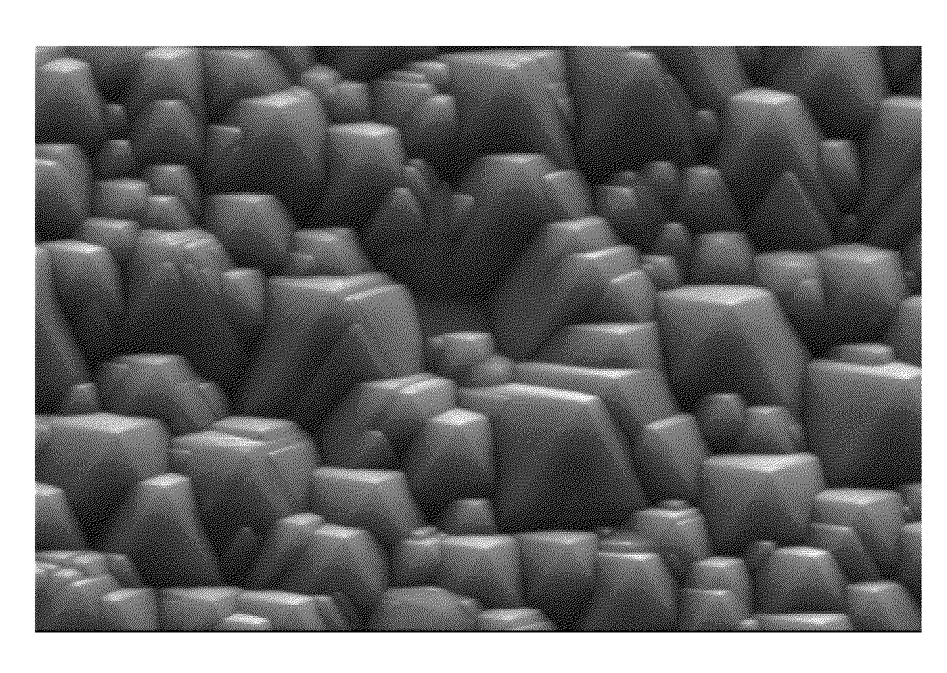
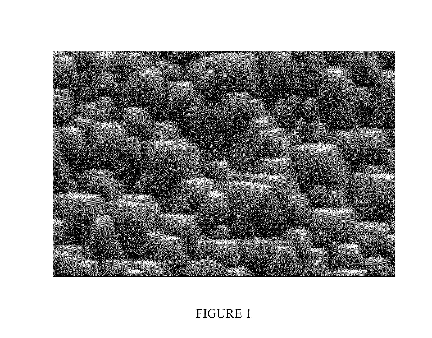
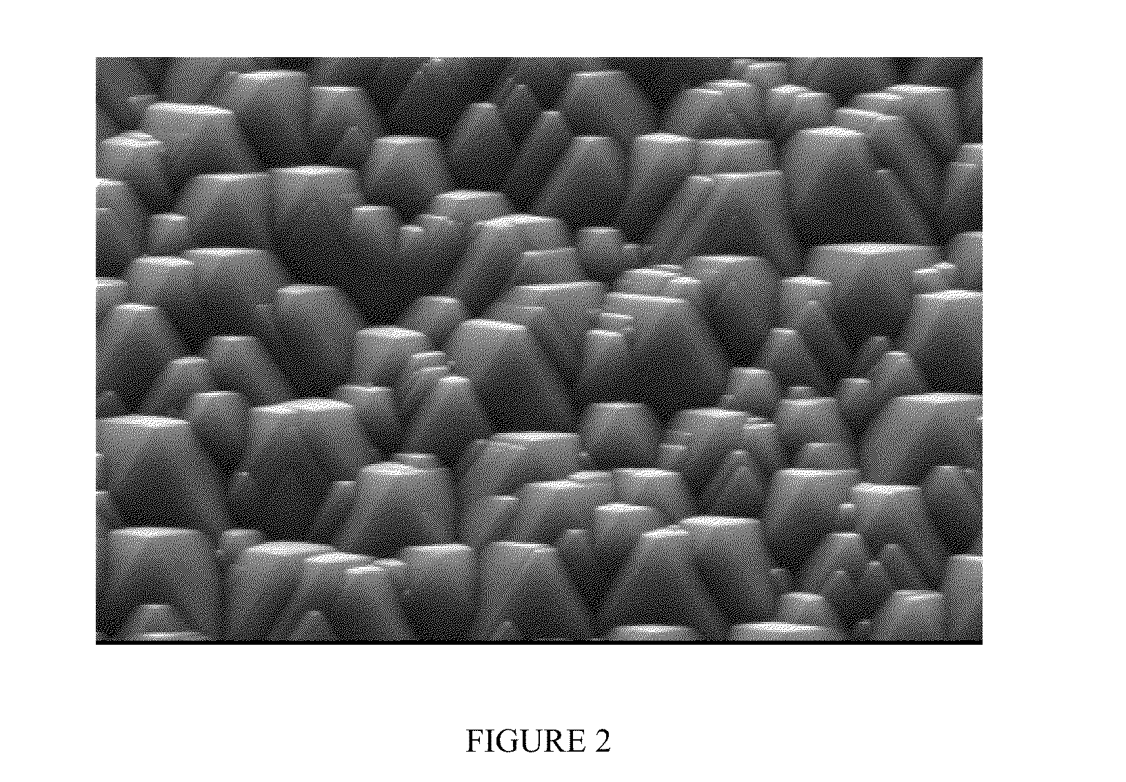
Image

Examples
example 1
[0052]Three doped monocrystalline silicon wafers (obtained from SolarGiga) having n+ doped zones on the front side or emitter layer and a pn-junctions below the emitter layer were immersed in an aqueous texturing solution in an 18 liter falcon line which is a large scale texturing bath. The texturing solution had the formula disclosed in Table 1 below.
TABLE 1COMPONENTAMOUNTTripropylene glycol10.5 wt %Potassium hydroxide 6 wt %1,4-butanediol20.5 wt %Water 93 wt %1weight average molecular weight = 192 g / mole;2Flash point = 121° C.flash point = 140.5° C.Boiling point = 268° C.
[0053]Each wafer was weighed before texturing. The aqueous texturing solution was at 80° C. There was no nitrogen bubbling. The solution was hand stirred. The pH of the texturing solution was 13. During texturing the dissolved oxygen content was measured using D0202G 2-Wire Dissolved Oxygen Analyzer (available from Yokogawa Electric Corporation). The average dissolved oxygen level for each wafer over its dwell ti...
example 2
[0057]The method described in Example 1 was repeated using three additional doped silicon monocrystalline semiconductor wafers. In addition to the components of Table 1, the aqueous texturing formulation included N-ispropylhydroxylamine. The aqueous texturing solution had the formulation shown in Table 3 below.
TABLE 3COMPONENTAMOUNTTripropylene glycol0.5wt %Potassium hydroxide6wt %1,4-butanediol0.5wt %N-isopropylhydroxylamine30.017wt %Water92.983wt %3Hydroguard ™ I-15 (available from The Dow Chemical Company, Midland, MI)
[0058]Each wafer was weighed before texturing and after texturing. The aqueous texturing solution was at 80° C. There was no nitrogen bubbling. The solution was hand stirred. The pH of the texturing solution was 13. The results are shown in Table 4.
TABLE 4Reflect-SiliconDissolvedanceRemovedOverallTestO2 Level% AverageStandardper SideAppearanceWafer(ppb)ReflectanceDeviation(μm)of Emitter4011.310.0411.61Completelyuniform5011.330.0711.55Completelyuniform6011.410.0111.4...
example 3
[0060]Two doped monocrystalline silicon semiconductor wafers were textured with one of the two texturing solutions shown in Table 5.
TABLE 5ComponentSolution 1Solution 2Tripropylene glycol1.2%bv1.2%bvPotassium hydroxide6wt %6wt %(25g / L)(25g / L)1,4-butanediol0.3%bv0.3%bvN-isopropylhydroxylamine00.017wt %WaterBalanceBalance
[0061]Each wafer was immersed in one of the two texturing solutions for 10 minutes. The solutions were kept at 80° C. and the pH of the solutions was at 13. There was no nitrogen bubbling and the solutions were hand stirred. The oxygen content of each bath was measured at the beginning of the texturing period using D0202G 2-Wire Dissolved Oxygen Analyzer. The oxygen content of solution 1 which did not include N-isopropylhydroxylamine had an oxygen content of 3.3 ppm. In contrast, solution 2 which included N-isopropylhydroxylamine had an oxygen content of 0 ppm.
[0062]The reflectance of each wafer was measured using a MacBeth Coloreye Reflectometer 7000 at a wavelength ...
PUM
| Property | Measurement | Unit |
|---|---|---|
| flash point | aaaaa | aaaaa |
| flash points | aaaaa | aaaaa |
| flash points | aaaaa | aaaaa |
Abstract
Description
Claims
Application Information
 - R&D
- Intellectual Property
- Life Sciences
- Materials
- Tech Scout
- Unparalleled Data Quality
- Higher Quality Content
- 60% Fewer Hallucinations
Browse by: Latest US Patents, China's latest patents, Technical Efficacy Thesaurus, Application Domain, Technology Topic, Popular Technical Reports.
© 2025 PatSnap. All rights reserved.Legal|Privacy policy|Modern Slavery Act Transparency Statement|Sitemap|About US| Contact US: help@patsnap.com