Nanotube phonon waveguide
- Summary
- Abstract
- Description
- Claims
- Application Information
AI Technical Summary
Benefits of technology
Problems solved by technology
Method used
Image
Examples
example 1
Preparation of a Nanotube Spanning a Heater and a Sensor Pad
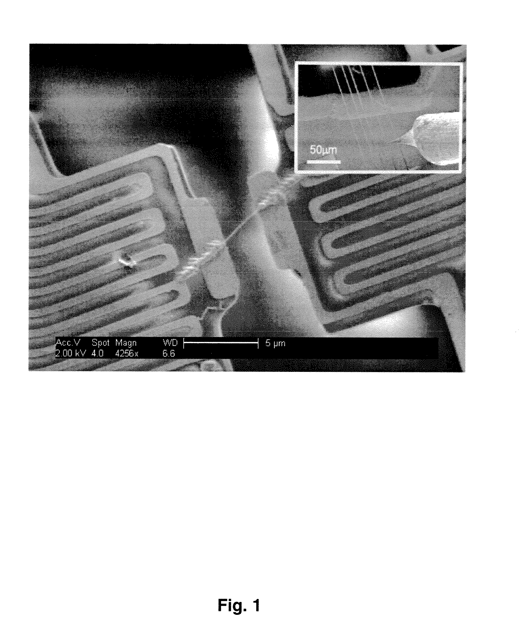
[0049]FIG. 1 shows a scanning electron microscopy (SEM) image of the central portion of a test fixture with a BNNT spanning the heat source / sink pads. Details of the test fixture fabrication process have been published elsewhere6. In brief, the fixture incorporates independently suspended heat source and heat sink pads, with integrated Pt film resistors serving symmetrically either as heaters or sensors (i.e., thermometers). In addition, two independent beams are used for resistance / thermopower measurements. The fixture was made adaptable to transmission electron microscopy (TEM) imaging by wet etching a window through the exposed Si below the sample mount region. As shown in FIG. 1, nanotubes were strongly bonded to the source / sink pads using (trimethyl)methylcyclopentadienyl platinum ((CH3)3(CH3C5H4)Pt) for mechanical strength and to reduce contact resistance.
[0050]For in-situ bending vs. electrical / thermal measurement, a...
example 2
Changes of Electrical Resistance, Thermopower, and Thermal Conductivity of a Nanotube During Deformation
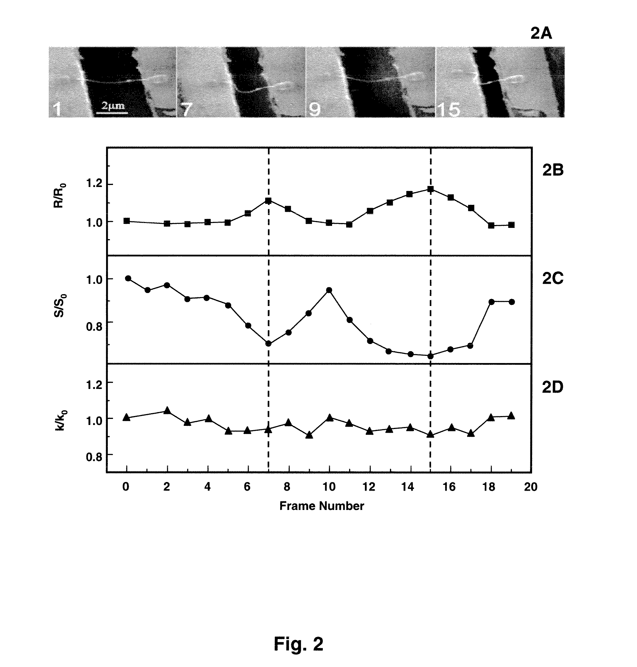
[0052]The upper part of FIG. 2 shows a series of representative SEM images with two cyclic bendings of CNT sample 1. The corresponding changes of the electrical resistance, thermopower, and thermal conductivity are shown in the lower part of FIG. 2. Their values are normalized to the initial quantities of 44 kΩ, −42 μV / K, and 1050 W / mK, respectively. The resistance shows a cyclic 20% modulation against deformation. It reaches maximum when the bending angle is largest, indicating a band-gap opening under deformation. Since the total conductance of a multiwall CNT is dominated by the metallic channels, FIG. 2B indicates that there is a metal to semiconducting transition when bending metallic tubes. The result is consistent with previous experiments7. It is also consistent with theoretical preconditions that suggest a band-gap opening when bending metallic CNTs8.
[0053]The total therm...
example 3
Insensitivity of Thermal Conductivity of MWCNTs by Cyclic Deformation
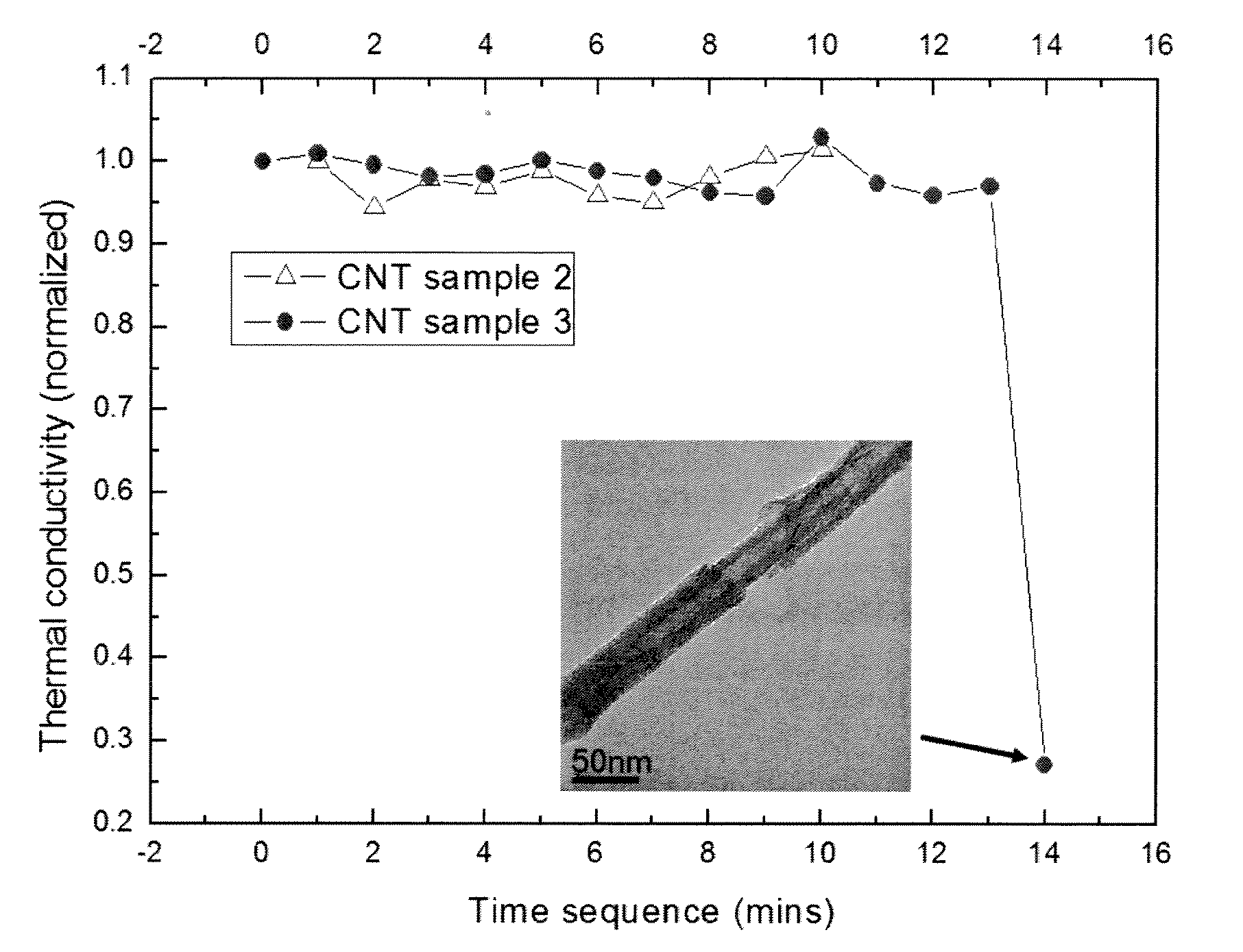
[0056]FIG. 3 shows two CNTs under cyclic deformation. The thermal conductivity is normalized to the initial values of 290 W / mK and 305 W / mK for CNT samples 2 and 3, respectively. At the extremes, the CNTs are bent at angles larger than 125° and 140°, respectively. Unlike FIG. 2, here the two CNTs are buckled locally so their radii of curvature are smaller (˜70 nm and ˜90 nm, for CNT samples 2 and 3, respectively). Remarkably, the thermal conductivity remains unchanged when the radius of curvature is comparable to their phonon mean free path (˜50 nm). As shown in the last data point of CNT sample 3, the thermal conductivity starts to decrease only when some permanent defects are created by suddenly releasing the device under strain. The TEM image in the inset of FIG. 3 clearly displays such defects.
[0057]To investigate whether this unique property is universal, we extended our study to BNNTs. BNNTs are known to have...
PUM
 Abstract
Description
Claims
Application Information
 - R&D
- Intellectual Property
- Life Sciences
- Materials
- Tech Scout
- Unparalleled Data Quality
- Higher Quality Content
- 60% Fewer Hallucinations
Browse by: Latest US Patents, China's latest patents, Technical Efficacy Thesaurus, Application Domain, Technology Topic, Popular Technical Reports.
© 2025 PatSnap. All rights reserved.Legal|Privacy policy|Modern Slavery Act Transparency Statement|Sitemap|About US| Contact US: help@patsnap.com


