Schottky diode integrated into LDMOS

a metal oxide semiconductor and diode technology, applied in the direction of semiconductor devices, electrical apparatus, transistors, etc., can solve the problems of high dynamic loss of ldmos, slow reverse recovery time, and loss of conduction loss in the inherent body diodes of the device, so as to reduce forward conduction loss, reduce leakage, and increase the safe operating area of ldmos

Inactive Publication Date: 2013-09-19
TEXAS INSTR INC
View PDF0 Cites 4 Cited by
  • Summary
  • Abstract
  • Description
  • Claims
  • Application Information

AI Technical Summary

Benefits of technology

[0006]According to the invention, there is provided an LDMOS device comprising a MOSFET and a Schottky diode integrated into the device adjacent the MOSFET. The MOSFET may include a lightly doped n-type region, typically in the form of an n-epitaxial region in which the n+ source is formed, and the Schottky diode may be formed by providing a metal or metalized region that forms a diode with the lightly doped n-type region. The metalized region may be a silicide region e.g., cobalt silicide. The silicide may be arranged to abut a lightly doped intermediate region that abuts the lightly doped n-type region. The MOSFET may be a butted source body device with a p-body and the n+ source formed in the same active region. The lightly doped n-type region may be an n-epitaxial region and the lightly doped intermediate region may be defined by the p-body, which may be contacted by means of at least one p+ body contact region. The source may be divided into multiple n+ source regions by intermediate p-body regions. In order to provide a junction between the silicide and the n-epitaxial region the n+ source regions may be blocked in the region defining the Shottky diodes. The MOSFET may include an n+ source and an n+ drain formed in the n-epitaxial region, the n-epitaxial region being formed on a p-type region, e.g. a p-substrate or p-epitaxial region grown on a substrate. The p+ body contact region, p−-body, and n+ source may be electrically tied together, e.g., by means of a common metal layer. The n+ source may include multiple n+ source regions separated by p-body regions to increase the safe operating area of the LDMOS. Each Schottky diode may be surrounded by a p+ ring for edge termination to reduce leakage. The p+ ring may be defined by the p+ contact region to the p-body.
[0007]Further, according to the invention, there is provided a method of reducing forward conduction loss in an LDMOS device, comprising integrating a Schottky diode with the LDMOS device. The LDMOS device may include a lightly doped n-type region and the Schottky diode may be formed by forming a metal or metalized region adjacent the lightly doped n-type region. The lightly doped n-type region may comprise an n-epitaxial region, which may be formed on a p-region e.g., a p-well region or p-body. The LDMOS device may include an n+ source and an n+ drain. The n+ source may include multiple n+ source regions, which may be separated by p-type regions, e.g., regions of a p-body. The metal or metalized region may comprise a silicided region, e.g., a cobalt silicide. In order to allow the silicided region to be formed adjacent the n-epitaxial region the formation of one or more of the n+ source regions may be blocked. The number of blocked n+ source regions can be increased to further reduce forward conduction loss. Typically the n+ source regions of an LDMOS are formed in a p-body, thus the silicide may be spaced from the n-epitaxial region by the p-body. The silicide region may be formed over the p-body.
[0008]Still further according to the invention, there is provided a method of reducing reverse recovery time in an LDMOS device, comprising integrating a Schottky diode with the LDMOS device. The LDMOS device may include a lightly doped n-type region and the Schottky diode may be formed by forming a metal or metalized region adjacent the lightly doped n-type region. The lightly doped n-type region may comprise an n-epitaxial region formed on a p-bulk. The LDMOS device may include an n+ source and an n+ drain. The n+ source may include multiple n+ source regions, which may be separated by regions of the p-body. The metal or metalized region may comprise a silicided region, e.g., a cobalt silicide. In order to allow the silicided region to be formed adjacent the n-epitaxial region the formation of one or more of the n+ source regions may be blocked. Typically the n+ source regions of an LDMOS are formed in a p-body, thus the silicide may be spaced from the n-epitaxial region by the p-body. The silicide region may be formed over the p-body.

Problems solved by technology

One of the drawbacks of an LDMOS device is the conduction loss in the inherent body diode of the device.
Also, due to minority carrier accumulation the reverse recovery time is slow.
Hence the LDMOS suffers from high dynamic losses due to the slow reverse recovery times.
However due to the high inductance of the package and printed circuit board the benefits are diminished.
The inductance of the external Schottky diode can be reduced by placing the Schottky diode in the same package as the MOSFET, however this requires two devices in the same package, which requires a large amount of space.

Method used


Image

  • Schottky diode integrated into LDMOS
  • Schottky diode integrated into LDMOS
  • Schottky diode integrated into LDMOS

Examples


Embodiment Construction

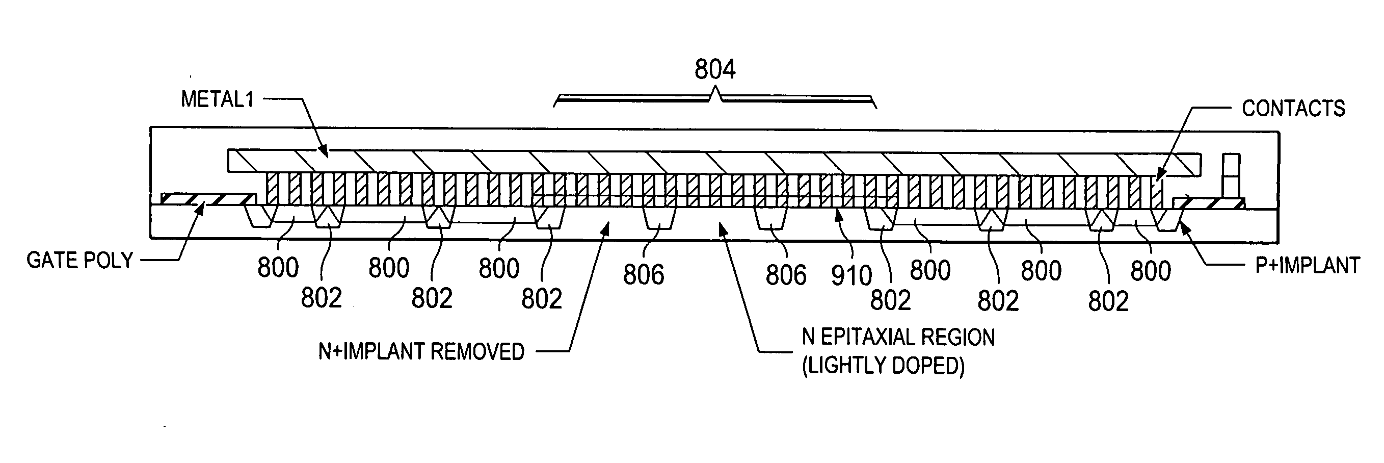
[0018]The present invention provides an LDMOS device with integrated Schottky diode.

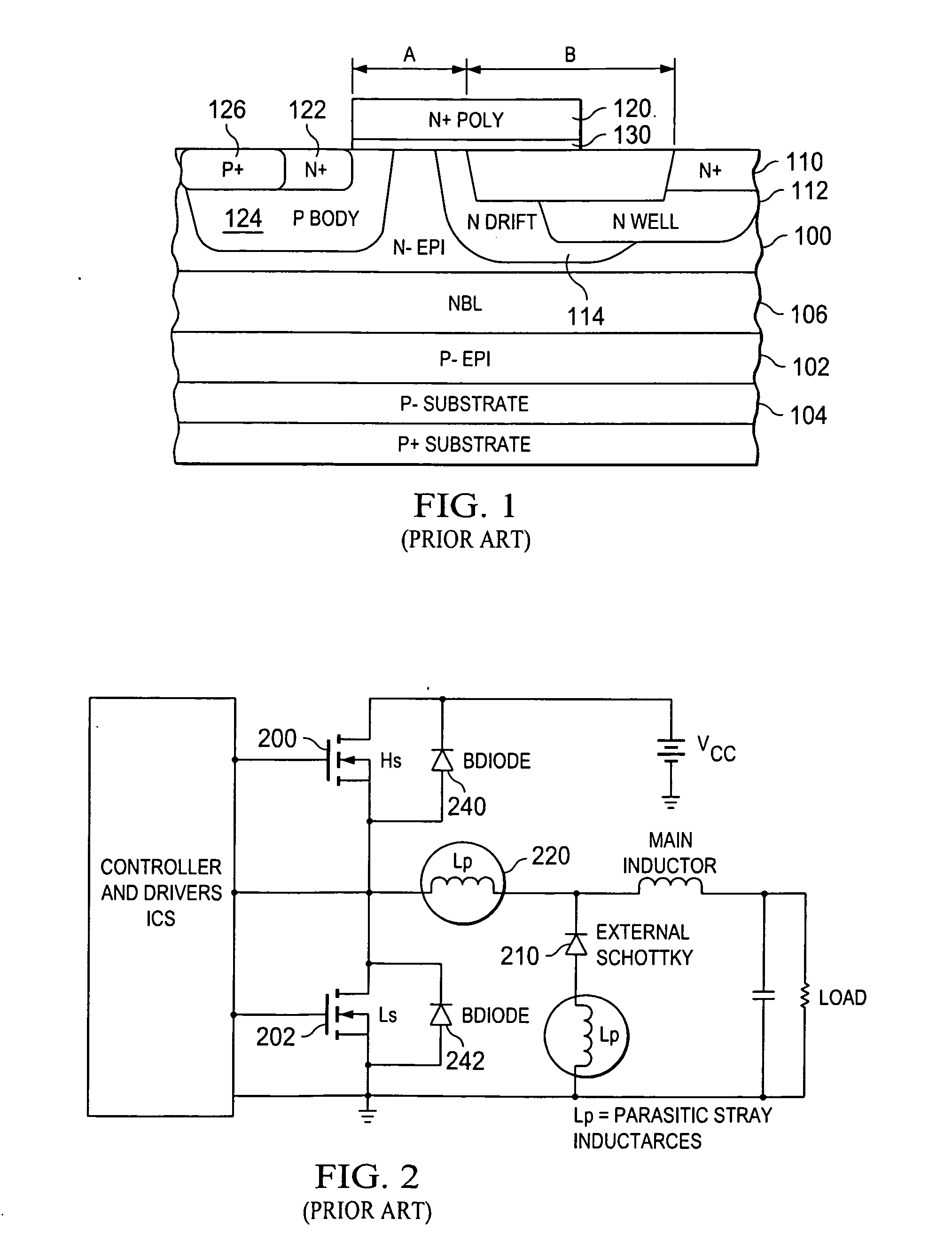
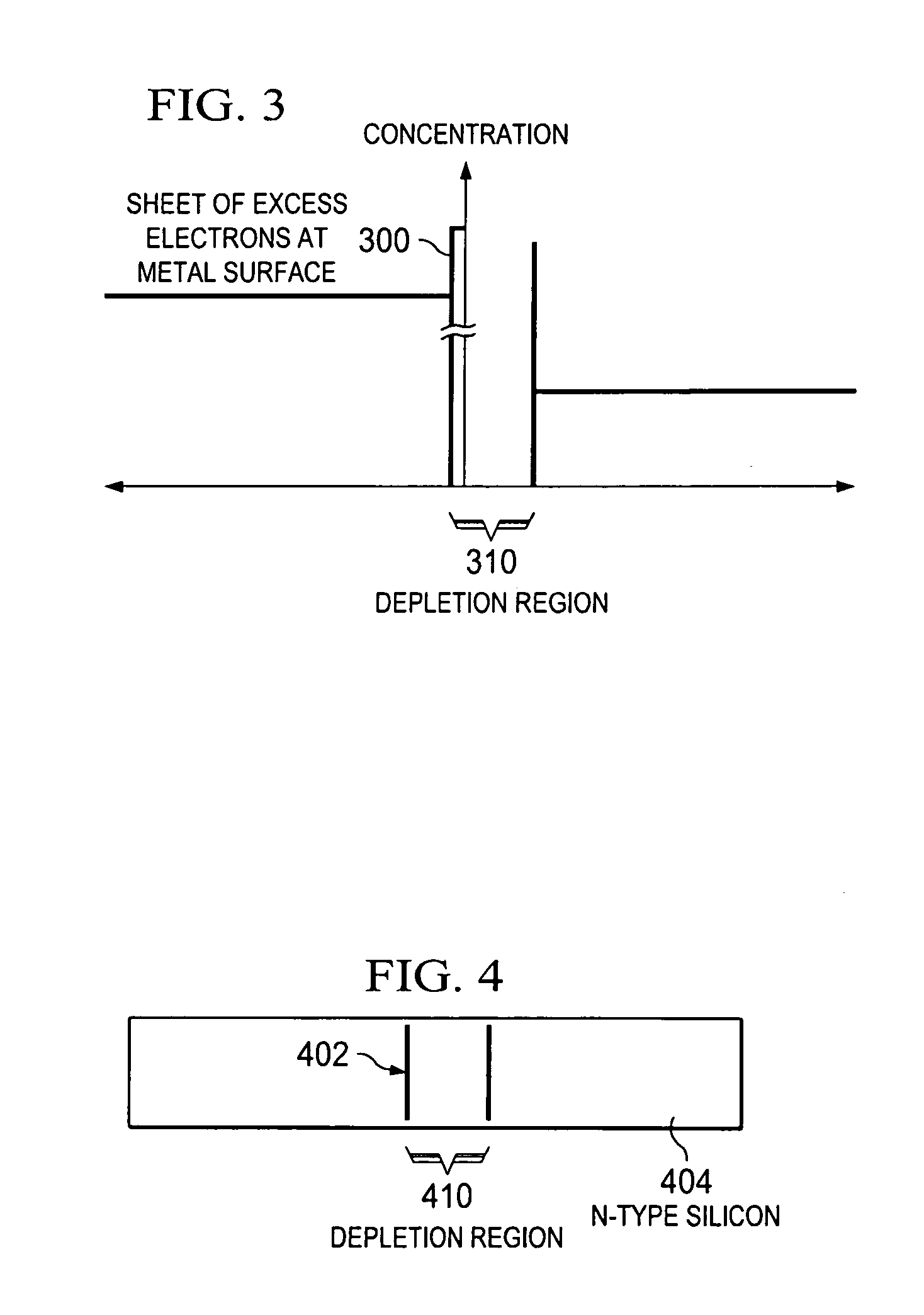
[0019]Schottky diodes are formed when a metal plate is brought into contact with lightly doped n-type silicon. As depicted in FIGS. 2 and 3, this creates a high concentration of electrons 300 at the surface 402 of the metal plate where it contacts the n-type silicon 404, and a depletion region 310, 410 between the metal plate and the n-type silicon, which shows the electron concentration across the Schottky diode. This provides the Schottky diode with a forward breakdown voltage Vf of about 0.3V compared to about 0.7V for a p-n diode formed between p-type silicon and n-type silicon. The benefits of a lower Vf are realized when the LDMOS is implemented in a circuit such as the buck converter of FIG. 2.

[0020]FIG. 5 shows the typical waveforms for a synchronous buck converter. As can be seen by comparing the voltage waveform on the gate of the high side LDMOS 100 (curve 500) with the voltage waveform on...


PUM


Abstract

In an LDMOS device leakage and forward conduction parameters are adjusted by integrating an Schottky diode into the LDMOS by blocking the formation of one or more n+ source regions and providing a metalized region adjacent to an underlying n-epitaxial region.

Description

FIELD OF THE INVENTION[0001]The invention relates to LDMOS (laterally diffused metal oxide semiconductor) devices. The invention is applicable to LDMOS which is used as a power switch (able to switch amperes of current). The requirements of a POWER MOSFET (like the LDMOS) are to minimize switching losses. In particular it relates to LDMOS devices implemented in a (Bipolar CMOS DMOS) BCD process.BACKGROUND OF THE INVENTION[0002]LDMOS (laterally diffused metal oxide semiconductor) transistors are commonly used in RF / microwave power amplifiers, e.g., in base-stations where the requirement is for high output power with a corresponding drain to source breakdown voltage usually above 60 volts. These transistors are fabricated by growing an epitaxial silicon layer on a more highly doped silicon substrate.[0003]A typical LDMOS is shown in FIG. 1, which shows a n-epitaxial layer 100 grown on a p-epitaxial layer 102, which, in turn is grown on a p-substrate 104. In this depiction, an n-buried...

Claims


Application Information

Patent Timeline
Patent Type & Authority Applications(United States)
IPC IPC(8): H01L27/06H01L21/329
CPCH01L29/41758H01L29/47H01L29/0878H01L29/0619H01L29/0696H01L29/782
Inventor RAGHAVAN, VENKATSTRACHAN, ANDREW D.
Owner TEXAS INSTR INC
Why Eureka
Try Eureka