Power semiconductor device with floating field ring termination

a technology of floating field ring and semiconductor device, which is applied in the direction of semiconductor device, basic electric element, electrical apparatus, etc., can solve the problems of significant technological constraints, complex analytical methods for designing ffr termination structures, and high computational effort, and achieve the effect of increasing the safe operating area

Active Publication Date: 2019-09-19
HITACHI ENERGY SWITZERLAND AG
View PDF0 Cites 1 Cited by
  • Summary
  • Abstract
  • Description
  • Claims
  • Application Information

AI Technical Summary

Benefits of technology

[0008]It is the object of the invention to provide a power semiconductor device comprising a floating field ring termination structure with an increased safe operating area.

Problems solved by technology

Given the well-known restrictions with SiC process technology, there are significant technological constraints.
This analytical method for designing a FFR termination structure is complex in that it requires a high computational effort especially for a high total number of floating field rings.
However, with regard to the safe operating area of the power semiconductor device, with this method optimum results cannot be achieved.
However, such design does also not result in optimum results with regard to the safe operating area of a power semiconductor device.

Method used


Image

  • Power semiconductor device with floating field ring termination
  • Power semiconductor device with floating field ring termination
  • Power semiconductor device with floating field ring termination

Examples


Embodiment Construction

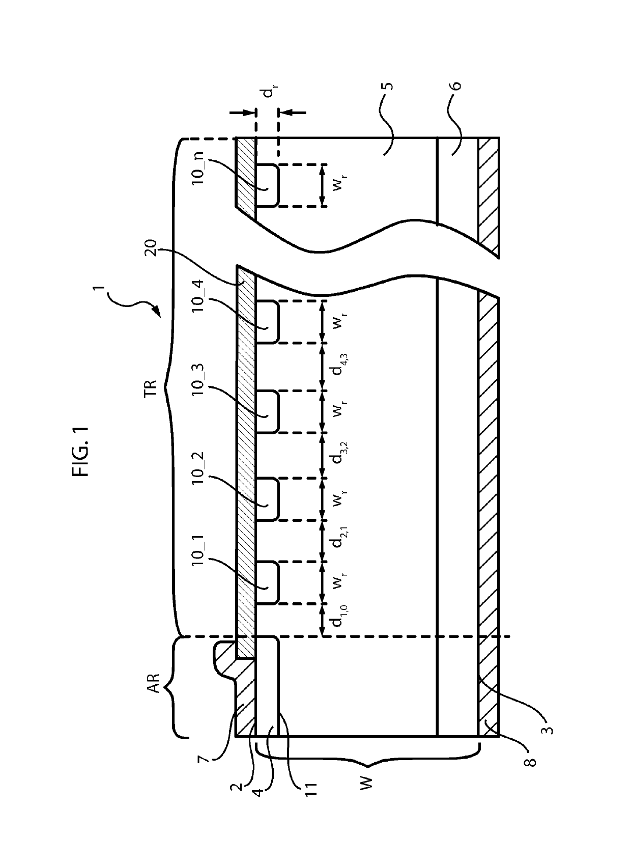
[0032]FIG. 1 is a partial cross-sectional view of a power semiconductor device 1 according to the invention. It comprises a semiconductor wafer W having a first main side surface 2 and a second main side surface 3, which is parallel to the first main side surface 2 and which is extending in a lateral direction. The wafer W has an active area AR and a termination area TR laterally surrounding the active area AR. In the order from the first main side surface 2 to the second main side surface 3, wafer W comprises a p-type anode layer 4, an n-type drift layer 5 and an n+-type substrate layer 6 having a doping concentration higher than that of the n-type drift layer 5. Exemplarily the doping concentration of the substrate layer 6 is 5·1018 cm−3 or more. The doping concentration of the anode layer 4 is exemplarily5·1016 cm−3 or more. The drift layer 5 is in direct contact with the anode layer 4 to form a main pn-junction 11. An anode electrode 7 is formed on the first main side surface 2 ...


PUM


Abstract

In a power semiconductor device of the application a total number n of floating field rings (10_1 to 10_n) formed in a termination area is at least 10. For any integer i in a range from i=2 to i=n, a ring-to-ring separation di,1−i between an i-th floating field ring and a directly adjacent (i−1)-th floating field ring, when counting the floating field rings (10_1 to 10_n) along a straight line starting from a main pn-junction and extending in a lateral direction away from the main pn-junction, is given by the following formula: di,i−1=d1,0j=1j=i−1 Δj for i=2 to n, wherein d1,0 is a distance between the innermost floating field ring (10_1) closest to the main pn-junction and the main pn-junction, and wherein: Δzone1−0.05·Δzone2jzone1+0.05·Δzone2 for j=1 to I-2, 2·Δzone2<zone2<Aj<Azonel +0.05 A zone2 <|Δj|<10·Δzone2. for j=I−1, 0.95·Δzone2j<1.05·Δzone2 for j=I to n−1, Δzone2<0.1 μm, and −Δzone2/2 <Δzone1zone2/2 , wherein I is an integer, for which 3≤l≤n/2.

Description

FIELD OF THE INVENTION[0001]The present invention relates to a power semiconductor device comprising a planar edge termination structure and in particular to a power semiconductor device comprising a floating field ring (FFR) termination (also called guard ring termination) in a termination region laterally surrounding an active region of a io wafer.BACKGROUND OF THE INVENTION[0002]Semiconductor devices, in particular power semiconductor devices, require an efficient edge termination to avoid electric field crowding at the edge of a main pn-junction resulting in breakdown of the device at a relatively low breakdown voltage VBR. Common power semiconductor devices, such as a pin diode or an insulated-gate bipolar transistor (IGBT), require an edge termination in order to achieve a breakdown voltage in the range of 80 to 90% of an ideal one-dimensional diode breakdown voltage.[0003]For silicon-based devices, known planar edge termination techniques include junction termination extensio...

Claims


Application Information

Patent Timeline
Patent Type & Authority Applications(United States)
IPC IPC(8): H01L29/861H01L29/868H01L29/06
CPCH01L29/0619H01L29/8611H01L29/868H01L29/872H01L29/1608H01L29/2003
Inventor BAUER, FRIEDHELMVEMULAPATI, UMAMAHESWARABELLINI, MARCO
Owner HITACHI ENERGY SWITZERLAND AG
Why Eureka
Try Eureka