
Resistive Switching Devices and Methods of Formation Thereof

a technology of resistive switching and switching device, applied in the field of resistive switching device, can solve the problems of significant threat to the continued advancement of memory technology, flash memory has a number of limitations, and current stand alone and embedded memory technology suffers many drawbacks

Active Publication Date: 2013-08-22
GLOBALFOUNDRIES US INC
View PDF17 Cites 83 Cited by
  • Summary
  • Abstract
  • Description
  • Claims
  • Application Information

AI Technical Summary

Benefits of technology

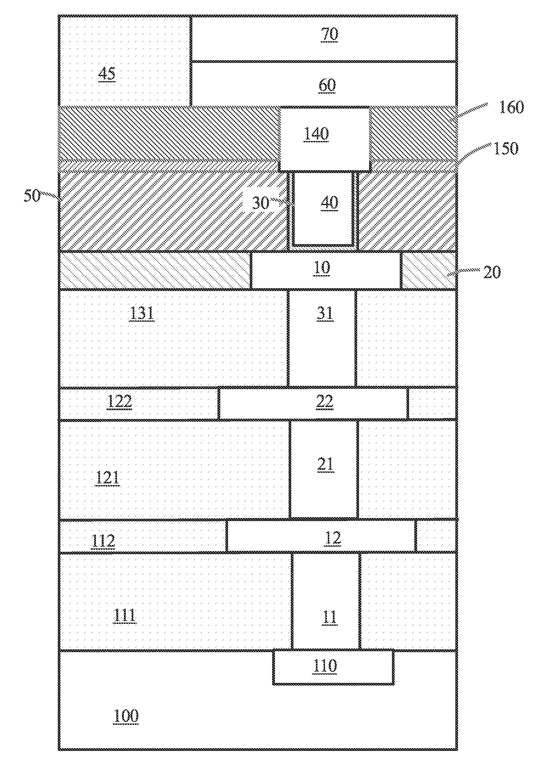
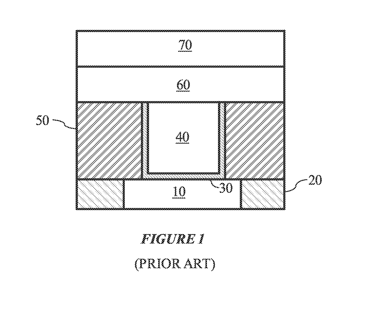
The present invention relates to a resistive switching device and a method of making it. The device has an opening in a first dielectric layer, with a conductive barrier layer on the sides and a fill material filling the opening. A solid electrolyte layer is formed on top of the opening, in contact with the fill material but not the conductive barrier layer. A top electrode is placed on top of the solid electrolyte. The technical effect of this invention is to provide a device with improved performance and stability.

Problems solved by technology

However, Flash memory has a number of limitations that is posing a significant threat to continued advancement of memory technology.
Current stand alone and embedded memory technologies suffer many drawbacks due to the extreme demands of scaling dictated by Moore's law.
Conventional non-volatile memories (NVM) technologies for both discrete and embedded applications require operational conditions that are incompatible with modern low voltage logic CMOS designs.
These requirements create complex integration issues as well as costly process and array concept especially for embedded NVM use models.

Method used


Image

  • Resistive Switching Devices and Methods of Formation Thereof
  • Resistive Switching Devices and Methods of Formation Thereof
  • Resistive Switching Devices and Methods of Formation Thereof

Examples


Embodiment Construction

[0021]The making and using of various embodiments are discussed in detail below. It should be appreciated, however, that the present invention provides many applicable inventive concepts that can be embodied in a wide variety of specific contexts. The specific embodiments discussed are merely illustrative of specific ways to make and use the invention, and do not limit the scope of the invention.

[0022]The present invention will be described with respect to various embodiments in a specific context, namely ionic switching devices such as programmable metallization cells (also called as conductive bridging memories, nanobridge memories, or electrolytic memories). The invention may also be applied, however, to other types of memories, particularly, to any two terminal resistive memory such as metal oxide memories and phase change memories. Although described herein for a memory device, the embodiments of the invention may also be applied to other types of devices formed by resistive sw...


PUM


Abstract

In accordance with an embodiment of the present invention, a resistive switching device includes an opening disposed within a first dielectric layer, a conductive barrier layer disposed on sidewalls of the opening, a fill material including an inert material filling the opening. A solid electrolyte layer is disposed over the opening. The solid electrolyte contacts the fill material but not the conductive barrier layer. A top electrode is disposed over the solid electrolyte.

Description

[0001]This application claims the benefit of U.S. Provisional Application No. 61 / 601,942, filed on Feb. 22, 2012, entitled “Semiconductor Devices and Methods of Formation Thereof,” which application is hereby incorporated herein by reference.TECHNICAL FIELD[0002]The present invention relates generally to electronic devices, and more particularly to resistive switching devices and methods of formation thereof.BACKGROUND[0003]The semiconductor industry demands that every new technology has to deliver increasing performance and density but with lower cost. Flash memory is the mainstream non-volatile memory in today's market. However, Flash memory has a number of limitations that is posing a significant threat to continued advancement of memory technology. Current stand alone and embedded memory technologies suffer many drawbacks due to the extreme demands of scaling dictated by Moore's law.[0004]Aggressive scaling has put the industry in such a predicament that only new materials, devi...

Claims


Application Information

Patent Timeline
IPC IPC(8): H01L45/00
CPCH01L45/085H01L45/1233H01L45/1253H01L45/142H01L45/143H01L45/144H01L45/065H01L45/147H01L45/08H01L45/16H01L21/06H01L21/04H01L45/146H01L21/76865H10N70/24H10N70/245H10N70/826H10N70/841H10N70/8822H10N70/8825H10N70/8828H10N70/8833H10N70/8836H10N70/011H10N70/235
Inventor GOPALAN, CHAKRAVARTHYSHIELDS, JEFFREYGOPINATH, VENKATESHWANG, JANET SIAO-YIANTSAI, KUEI-CHANG
Owner GLOBALFOUNDRIES US INC
Learn More