Iii nitride epitaxial substrate and deep ultraviolet light emitting device using the same
a technology of nitride epitaxial substrate and deep ultraviolet light, which is applied in the direction of semiconductor/solid-state device manufacturing, semiconductor devices, electrical devices, etc., can solve the problems of iii nitride semiconductor cracks and pits (point-like defects), and achieve the effect of improving light output power and improving light output power
- Summary
- Abstract
- Description
- Claims
- Application Information
AI Technical Summary
Benefits of technology
Problems solved by technology
Method used
Image
Examples
example 1
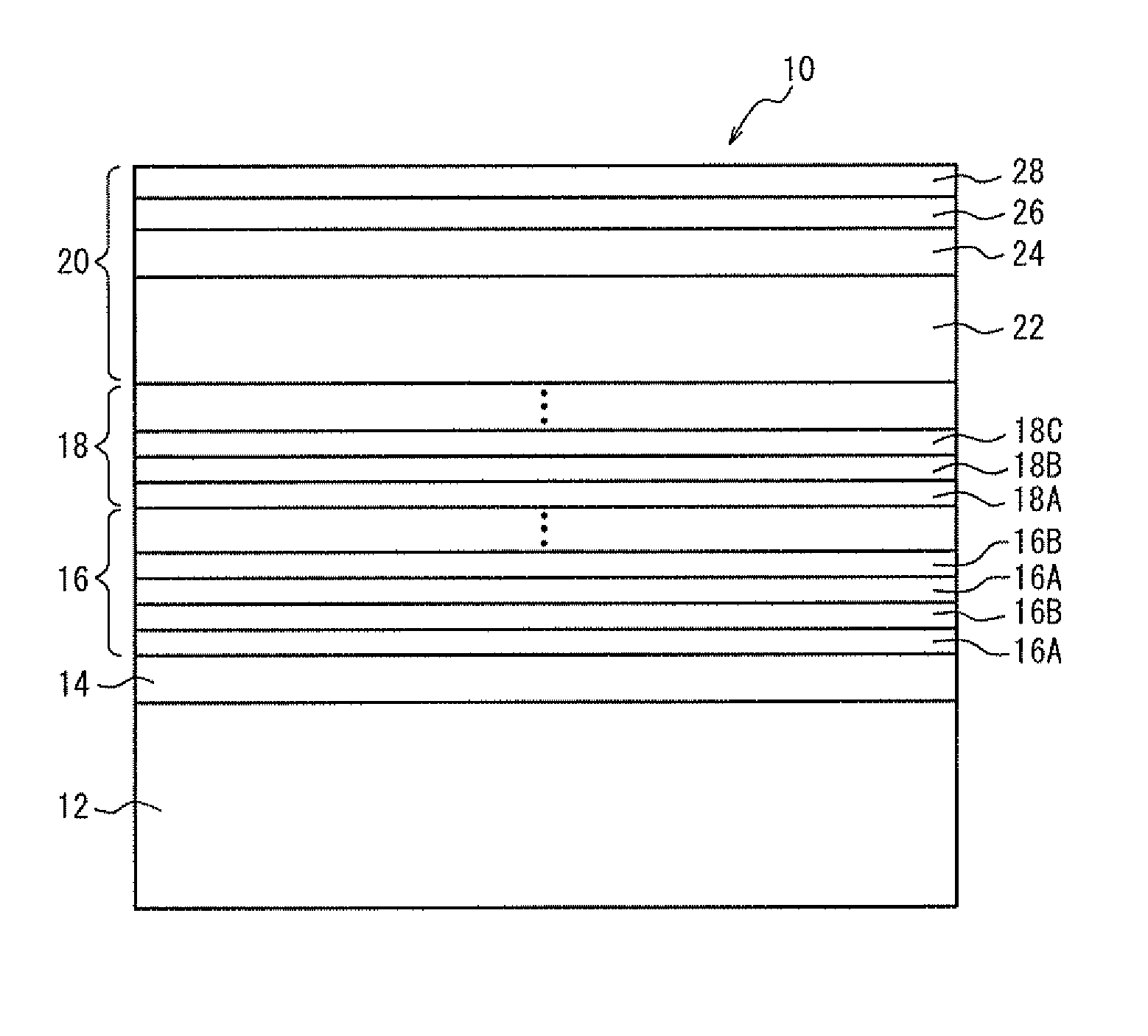
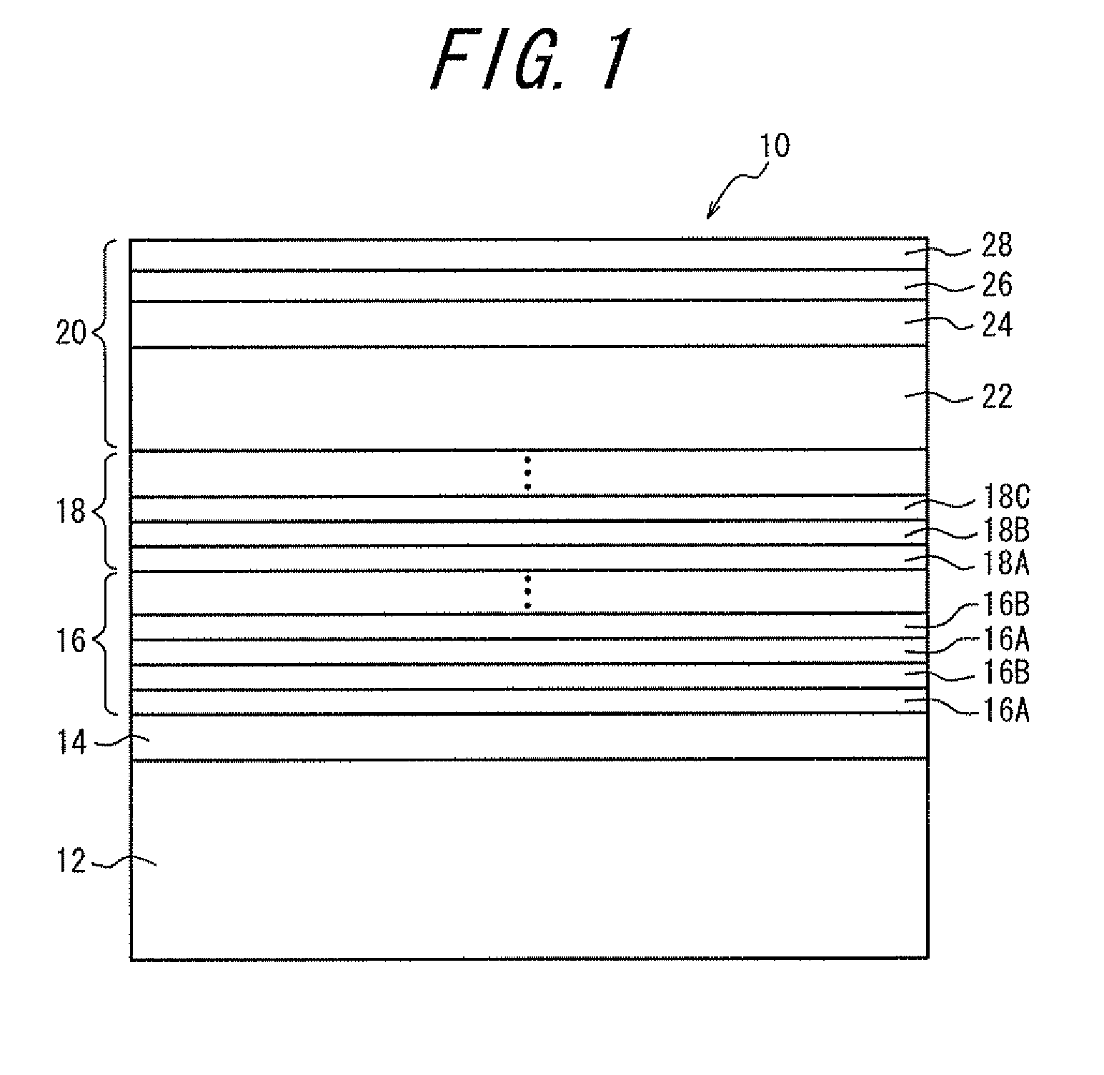
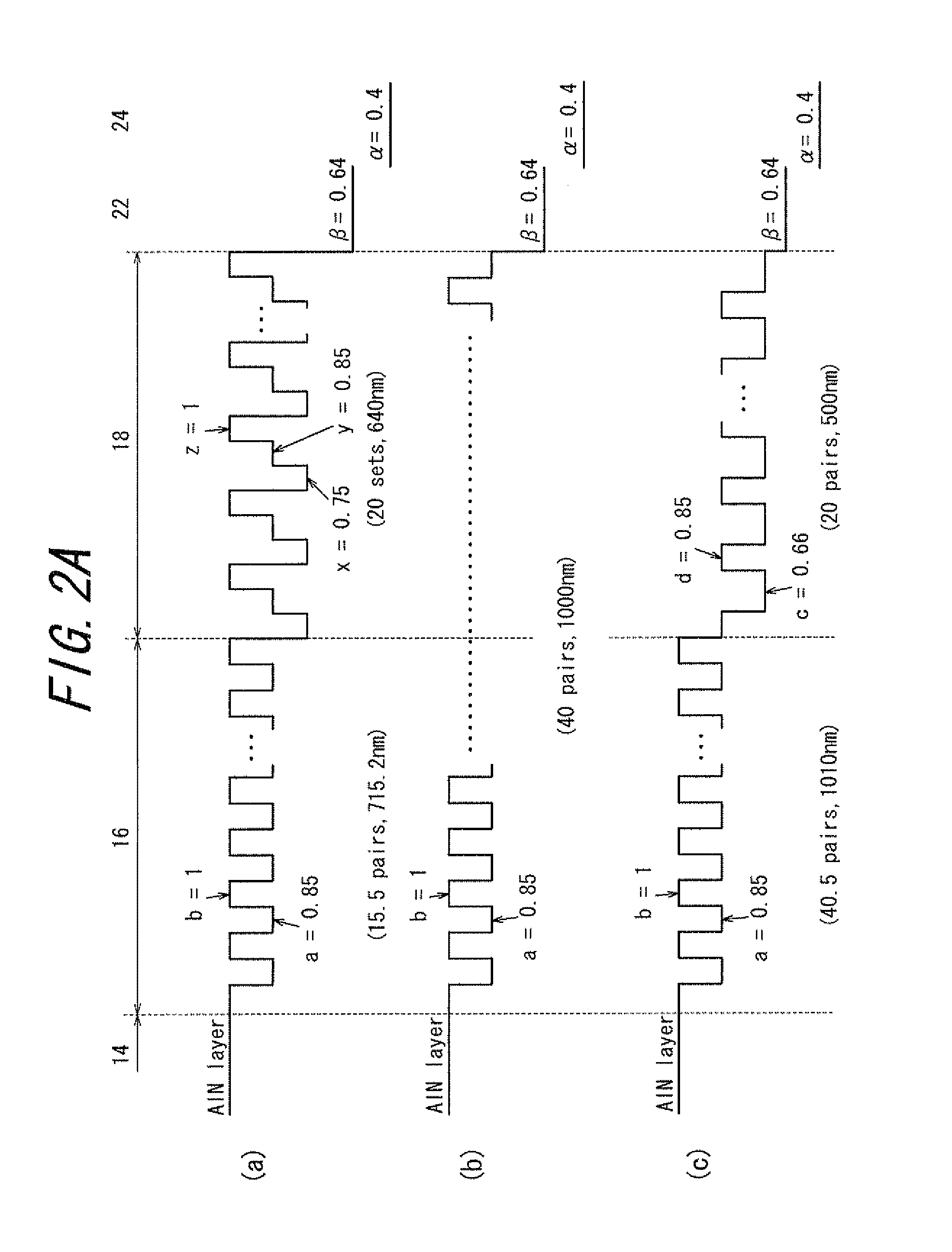
[0065]An AlN template substrate was prepared in which an AlN layer (thickness: 0.8 μm) was formed as a buffer layer on a sapphire substrate (thickness: 430 μm). A first superlattice laminate and a second superlattice laminate shown in FIG. 2A, section (a) were epitaxially grown sequentially on this AlN template substrate. The first superlattice laminate includes first layers (Al0.85Ga0.15N, a=0.85, thickness: 40 nm) and second layers (AlN, b=1, thickness: 7.2 nm) which are alternately stacked. One of the second layers was first formed on the AlN template substrate, and then 15 pairs of the first layers and the second layers were stacked thereon. Accordingly, the layers are collectively expressed as 15.5 pairs in FIG. 2, section (a). The second superlattice laminate includes 20 repeated layer sets of third layers (Al0.75Ga0.25N, x=0.75, thickness: 4 nm), fourth layers (Al0.85Ga0.15N, y=0.85, thickness: 17 nm), and fifth layers (AlN, z=1, thickness: 11 nm) which are stacked in this or...
example 2
[0067]A III nitride epitaxial substrate of Example 2 was fabricated by the same method to that used in Example 1 except that the number of the layer sets in the second superlattice laminate was changed to 40.
example 3
[0073]This example is the same to Example 1 except that a III nitride epitaxial substrate with an emission wavelength of 340 nm was fabricated by epitaxially growing an n-type AlGaN layer (Al content β: 0.29, thickness: 1680 nm, dopant: Si), an active layer (AlGaN-based MQW layer, thickness: 290 nm, Al content α in the well layer: 0.03), a p-type AlGaN layer (a composition graded layer having an Al content of 0.49 to 0.32, thickness: 80 nm, dopant: Mg), and a p-type GaN contact layer (thickness: 66 nm, dopant: Mg) sequentially on the second superlattice laminate of Example 1.
PUM
 Abstract
Description
Claims
Application Information
 - R&D
- Intellectual Property
- Life Sciences
- Materials
- Tech Scout
- Unparalleled Data Quality
- Higher Quality Content
- 60% Fewer Hallucinations
Browse by: Latest US Patents, China's latest patents, Technical Efficacy Thesaurus, Application Domain, Technology Topic, Popular Technical Reports.
© 2025 PatSnap. All rights reserved.Legal|Privacy policy|Modern Slavery Act Transparency Statement|Sitemap|About US| Contact US: help@patsnap.com


