
Embedded stressors for multigate transistor devices

a multi-gate transistor and stressor technology, applied in the field of multi-gate transistor devices, can solve the problems of increasing power consumption in idle state, increasing efficiency of effect transistors (fets), and increasing inefficiency of nanometer devices, and achieve the effect of improving the mobility of charge carriers in the channel region

Active Publication Date: 2013-06-20
TOAGOSEI CO LTD
View PDF4 Cites 37 Cited by
  • Summary
  • Abstract
  • Description
  • Claims
  • Application Information

AI Technical Summary

Benefits of technology

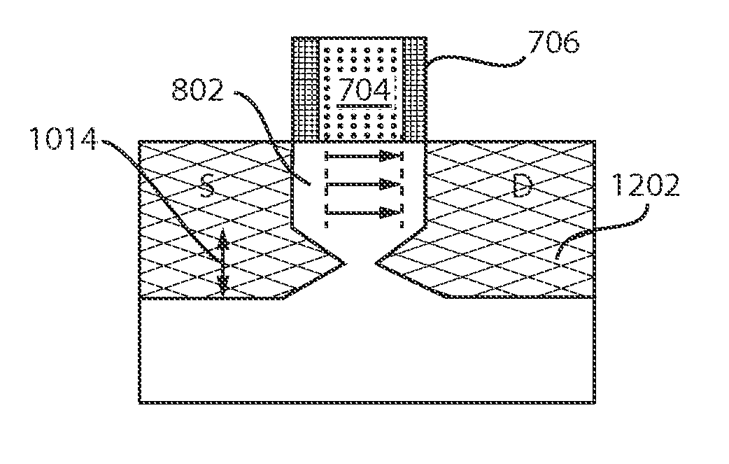
The patent text describes a method for fabricating a multigate transistor device with a recessed portion below the gate structure that enhances charge carrier mobility in the channel region. The recessed portion includes at least one angled indentation and a source and drain extension that extends into the indentation and provides a stress on the channel region. The device also includes a circuit apparatus with a plurality of multigate devices and a gate structure, where the terminal extensions form a cohesive lattice structure that provides stresses on the channel regions. The technical effect is improved charge carrier mobility in the channel region.

Problems solved by technology

Planar field-effect transistor (FET) devices, which have been widely used in integrated circuits for the past several decades, were found to be increasingly inefficient on the nanometer scale.
Reducing the size of the channel between the terminals of planar transistors to this scale leads to an inefficient leakage of current in the off-state of the transistor, resulting in an increase in power consumption in its idle state.

Method used


Image

  • Embedded stressors for multigate transistor devices
  • Embedded stressors for multigate transistor devices
  • Embedded stressors for multigate transistor devices

Examples


Embodiment Construction

[0026]Multigate devices provide an excellent building block for nanometer scale integrated circuit designs due to their effectiveness in the suppression of leakage current. However, to meet increasing demands for computing devices with low power consumption, the energy consumption of integrated circuit elements should be reduced as much as possible. The energy efficiency of multigate devices can be improved by reducing resistance in the channel regions and at the source and drain regions of the devices. For example, the series resistance at the source and drain regions of multigate devices can be reduced by merging the fins of such devices through a selective, epitaxial growth of undoped silicon, doped silicon, doped SiGe, or other suitable materials, in regions between the fins. Moreover, the resistance in the channel region of the multigate device can be reduced through the imposition of appropriate stresses. For example, the introduction of a tensile stresses to the channel regio...


PUM


Abstract

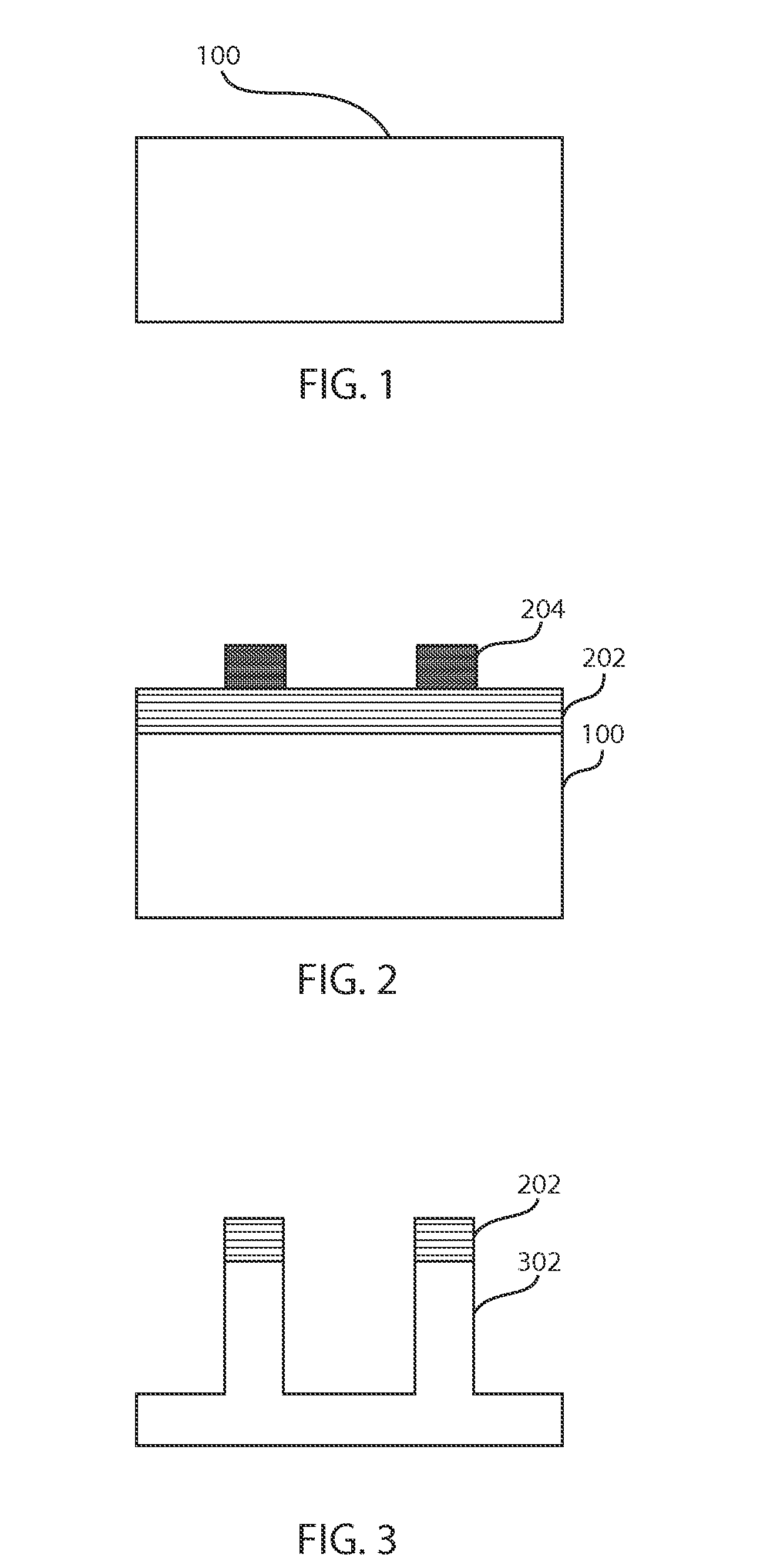
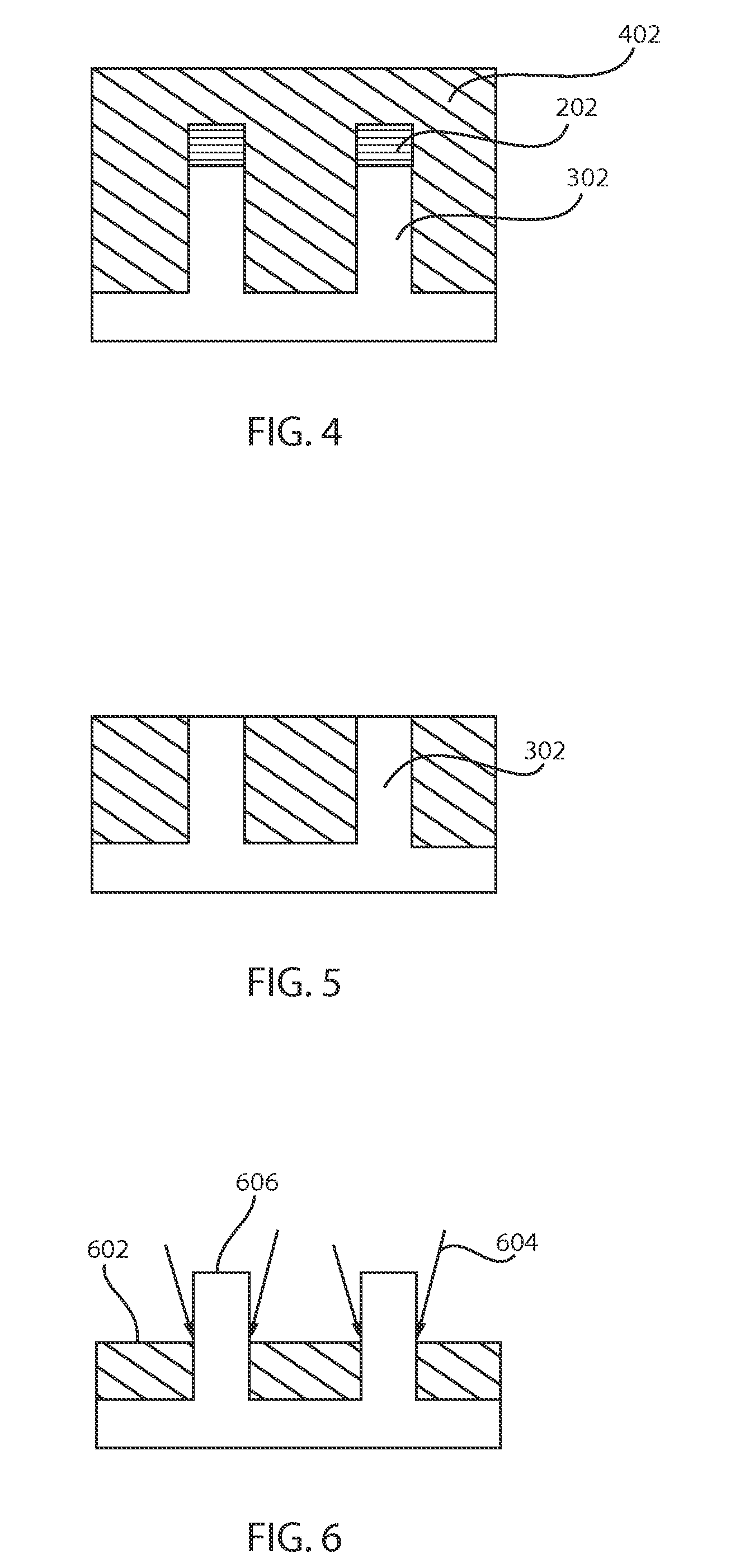
Multigate transistor devices and methods of their fabrication are disclosed. In accordance with one method, a fin and a gate structure that is disposed on a plurality of surfaces of the fin are formed. In addition, at least a portion of an extension of the fin is removed to form a recessed portion that is below the gate structure, is below a channel region of the fin, and includes at least one angled indentation. Further, a terminal extension is grown in the at least one angled indentation below the channel region and along a surface of the channel region such that the terminal extension provides a stress on the channel region to enhance charge carrier mobility in the channel region.

Description

RELATED APPLICATION DATA[0001]This application is a Continuation application of co-pending U.S. patent application Ser. No. 13 / 325,506 filed on Dec. 14, 2011, incorporated herein by reference in its entirety.BACKGROUND[0002]1. Technical Field[0003]The present invention relates to transistor devices, and, more particularly, to multigate transistor devices and systems, and methods of their fabrication and use.[0004]2. Description of the Related Art[0005]Throughout the evolution and advancement of computing devices, the reduction of their size and their power consumption in a way that maintains or improves a high processing capacity has long been a design goal. Planar field-effect transistor (FET) devices, which have been widely used in integrated circuits for the past several decades, were found to be increasingly inefficient on the nanometer scale. Reducing the size of the channel between the terminals of planar transistors to this scale leads to an inefficient leakage of current in ...

Claims


Application Information

Patent Timeline
IPC IPC(8): H01L29/78
CPCH01L29/66795H01L29/165H01L29/7848H01L29/785H01L29/7853
Inventor CAI, MINGGUO, DECHAOKULKARNI, PRANITAYEH, CHUN-CHEN
Owner TOAGOSEI CO LTD
Learn More