Image Sensor Module Package and Manufacturing Method Thereof

a technology of image sensor and module, applied in the direction of electrical apparatus, semiconductor devices, radio frequency control devices, etc., can solve the problems of reducing electrical and thermal performance, bad reliability, etc., and achieve the effect of easy peeling

Inactive Publication Date: 2013-05-23
TONG HSING ELECTRONICS INDS
View PDF5 Cites 6 Cited by
  • Summary
  • Abstract
  • Description
  • Claims
  • Application Information

AI Technical Summary

Benefits of technology

[0009]A main object of the present invention is to provide an image sensor module package, wherein a relatively large soldering area is provided through at least one groove at a lateral side of an insulating layer, so that an desired effect, that the image sensor module package being firmly bonded to a system-level printed circuit board by a soldering and not being easy to peel off, is achieved.

Problems solved by technology

Unlike the conventional art, the holes are completely filled with metal to form a metal column having electrically conducting ability, wherein during the plating procedure, trapped voids and solutions are easily produced, thereby they are not only difficult to be release out and may bring down the electrically and thermally performances, but also result in a bad reliability.

Method used


Image

  • Image Sensor Module Package and Manufacturing Method Thereof
  • Image Sensor Module Package and Manufacturing Method Thereof
  • Image Sensor Module Package and Manufacturing Method Thereof

Examples


Embodiment Construction

[0048]The following description is disclosed to enable any person skilled in the art to make and use the present invention. Preferable embodiments are provided in the following description only as examples and modifications will be apparent to those skilled in the art. The general principles defined in the following description would be applied to other embodiments, alternatives, modifications, equivalents, and applications without departing from the spirit and scope of the present invention.

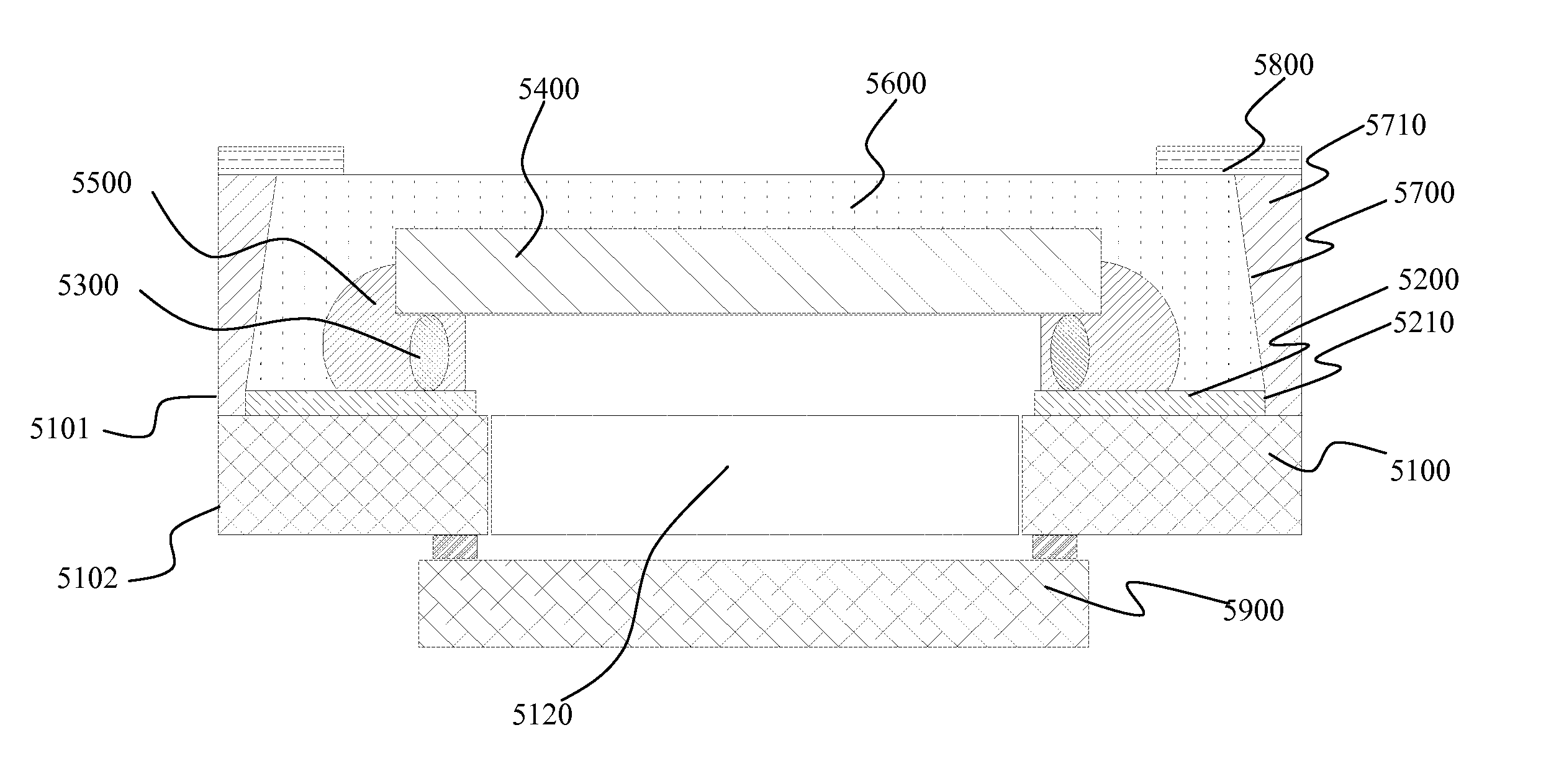
[0049]FIG. 1 is a top view of an image sensor module package according to a first preferred embodiment of the present invention. One or more grooves 1700 are provided around an outer circumference of an insulating layer 1600. A metal layer 1710 is provided in each of the grooves 1700 and has a portion protruded from the insulating layer 1600 to perform as an output / input contact.

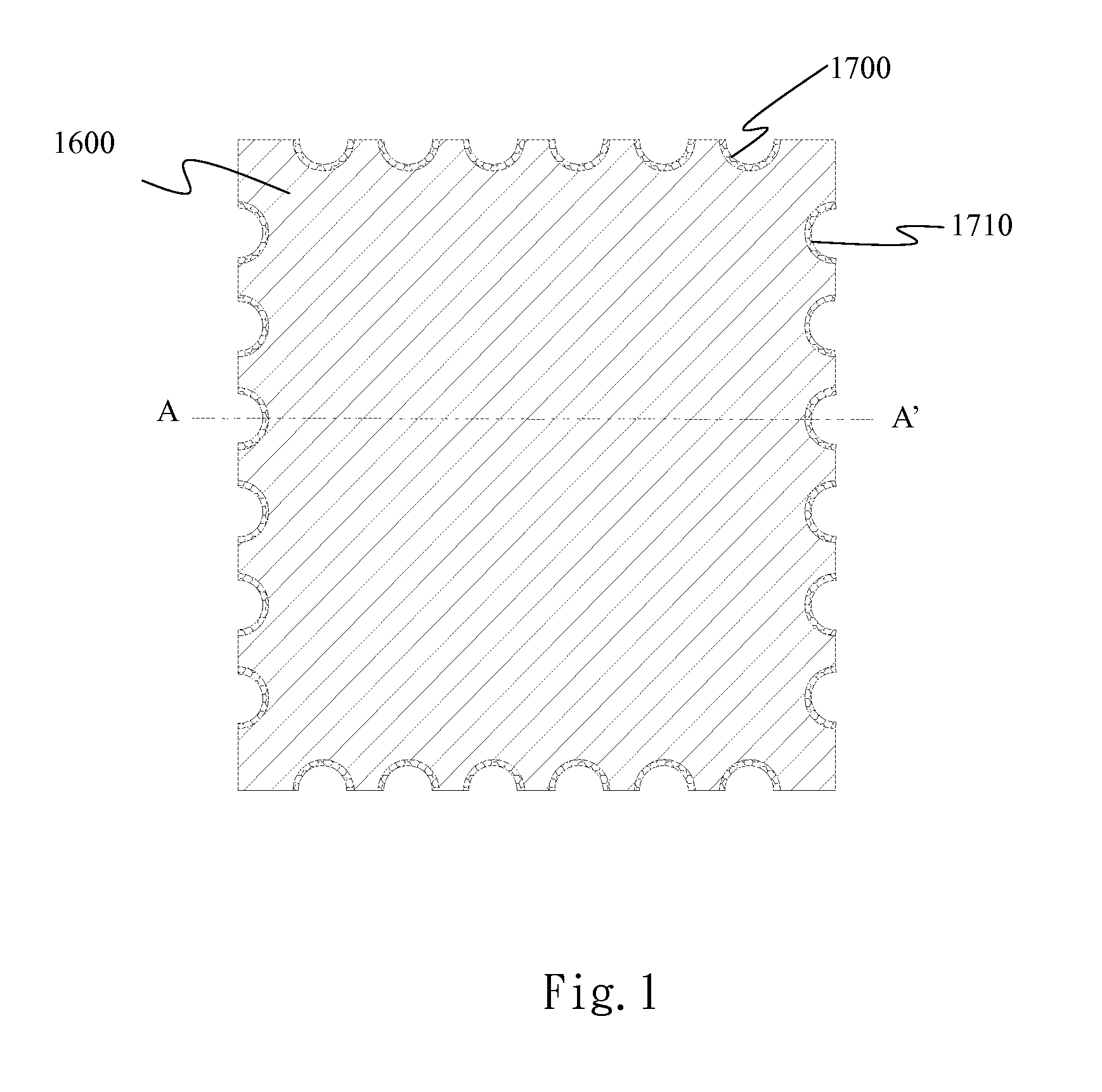
[0050]FIG. 2 is a sectional view along line A-A in FIG. 2 illustrating the image sensor module package according to th...


PUM


Abstract

An image sensor module includes a substrate, a circuit layer, a flip chip, an insulating layer, and a conducting layer. The substrate has at least one transparent area and defines a first surface and a second surface. The circuit layer is provided on the first surface of the substrate. The flip chip is connected to the circuit layer. The insulating layer substantially encases the flip chip and a part of the circuit layer, wherein the insulating layer has at least one groove at a lateral side of said insulating layer thereof each provided with a metal layer. The conducting layer is provided on a top surface of the insulating layer, wherein the conducting layer is electrically connected to the circuit layer via the metal layer.

Description

NOTICE OF COPYRIGHT[0001]A portion of the disclosure of this patent document contains material which is subject to copyright protection. The copyright owner has no objection to any reproduction by anyone of the patent disclosure, as it appears in the United States Patent and Trademark Office patent files or records, but otherwise reserves all copyright rights whatsoever.BACKGROUND OF THE PRESENT INVENTION[0002]1. Field of Invention[0003]The present invention relates to sensor module package and a manufacturing method thereof, and more particularly to an image senor module package and a manufacturing method thereof.[0004]2. Description of Related Arts[0005]A conventional image sensor module package employs a wire bonding technology to electrically connect a chip with a printed circuit board. Accordingly, an image sensor chip is provided on a ceramic substrate, wherein the image sensor chip is electrically connected to the ceramic substrate in a wire bonding manner, and then a glass l...

Claims


Application Information

Patent Timeline
Patent Type & Authority Applications(United States)
IPC IPC(8): H01L31/02
CPCH01L27/14683H01L27/14618H01L2924/0002H01L2924/00
Inventor RU, SHAO-PIN
Owner TONG HSING ELECTRONICS INDS
Why Eureka
Try Eureka