
Method to perform electrical testing and assembly of electronic devices

a technology for electronic devices and assembly, applied in the direction of individual semiconductor device testing, semiconductor/solid-state device testing/measurement, instruments, etc., can solve the problems of wire detachment from the pad, damage to the latter, and big problems

Active Publication Date: 2013-05-02
STMICROELECTRONICS SRL
View PDF2 Cites 5 Cited by
  • Summary
  • Abstract
  • Description
  • Claims
  • Application Information

AI Technical Summary

Benefits of technology

The method described in this patent allows for the testing and assembly of electronic devices on a wafer with minimal damage to the pads or bumps of the chips. This method is simple and low-cost, and it overcomes limitations and drawbacks associated with previous methods. Additionally, the patent describes a technique for creating an electronic device by cutting the wafer and extending the metallization layer to the edge of the device.

Problems solved by technology

The use of probes that are positioned on the pads to electrically connect the tester to the wafer implies a damaging of the metal the pads are made of, creating big problems, not only during the testing or “probing”, but especially during the assembly of the die.
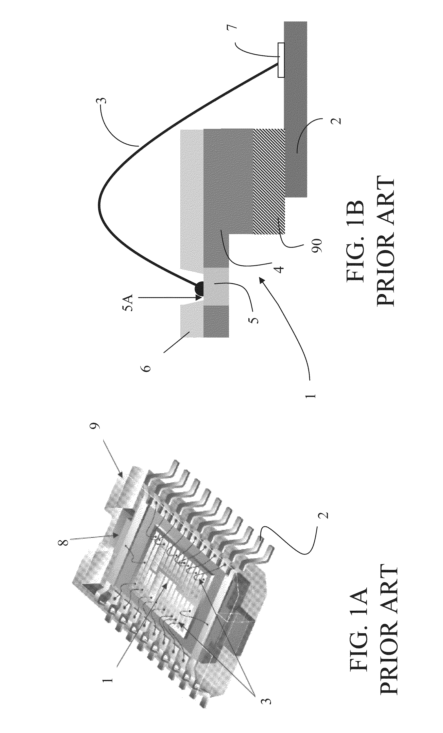
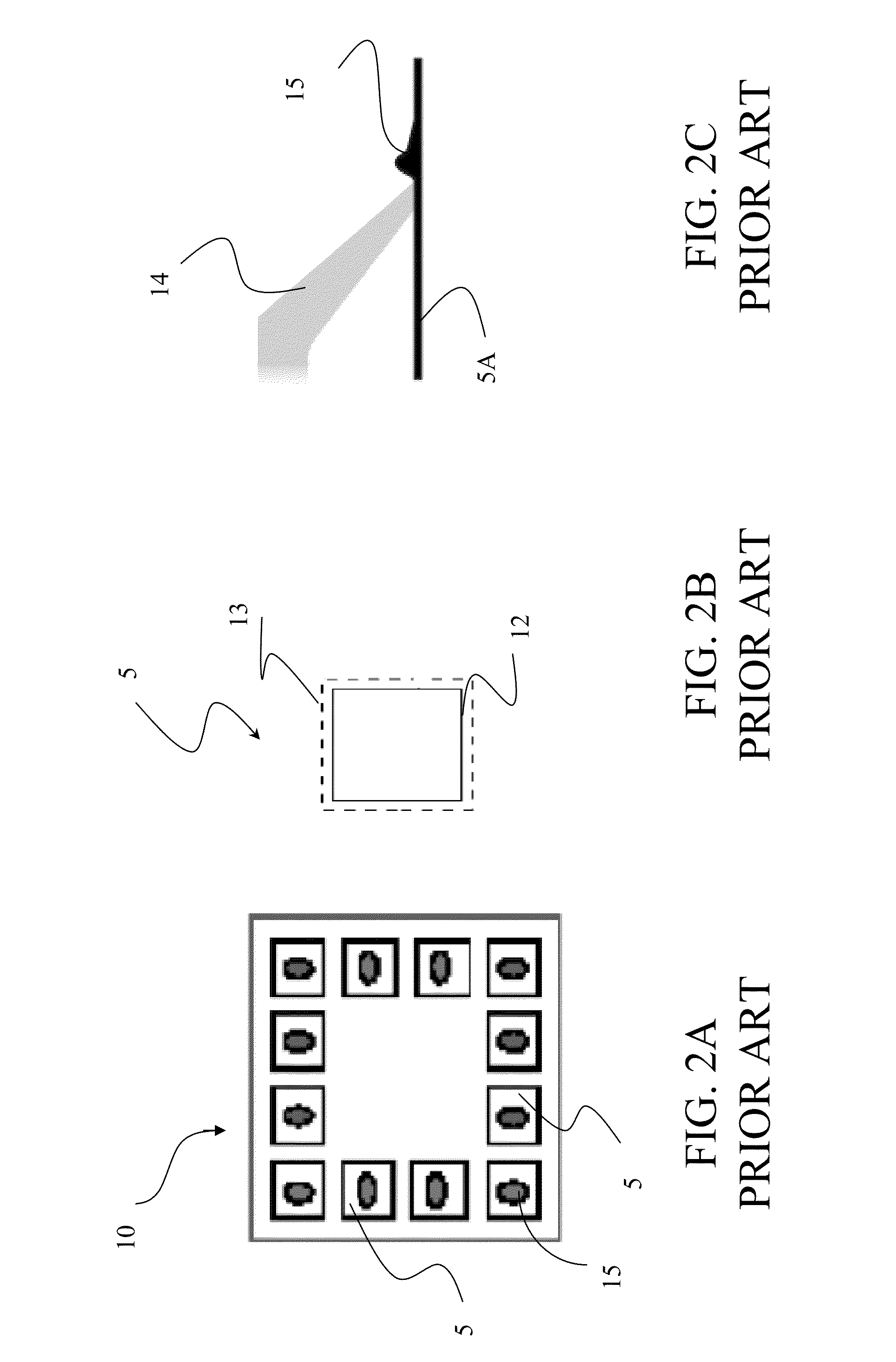
If the probes of a probe card are placed on the pad 5, this latter can be damaged.
In particular, this damaging of the surface of the pad can imply a poor adhesion of the bonding metallic wire to the damaged surface, causing the detachment of the wire from the pad, or even a total lack of adhesion and, thus, the impossibility of creating an electric connection through wire bonding.
A further problem arises, when more dice should be embedded inside a package in “stacked” configurations for example of the pyramidal (pyramidal stacked), symmetrical (twin stacked), or with rotated overlapping (overhanging stacked) types, which consist in stacking different dice of different size one above the other, and then creating the connections between the dice and between die and support element of the package through wire bonding.
In fact, in this type of configuration it often occurs that the sizes of the upper die are limited to the position of the pads and of the corresponding wire bonding of the die.
A further problem arises during the performance of a testing of more devices in parallel, for which probe cards with a very high number of probes may be used.
This determines an increase of the contacting problems and, thus, of electrical continuity, between the probe card and the wafer, i.e., between the probes and pads of the device to be tested, which causes successive probing on the same devices.
Although the Studded Pad is advantageous in terms of protection of the layers underlying the pad, to form the protection oxide grid of the copper metallization layer, additional process steps are involved, which consequently burden and complicate the manufacturing of the device.
A further problem of the performance of a probing through probes is represented by the mechanical limits of the devices of last generation, which have a high number of pads to be contacted or pads with reduced area or also pads very close to each other, i.e., with reduced “pitch” or “fine pitch”.
In fact, in case of pads with reduced size and of a high temperature of the wafer, for example much higher than 25 degrees centigrade, it can occur that at least one probe of the probe card, after having contacted the pad, moves on the pad itself due to the thermal expansion of the probe card, causing the breakage of the passivation layer surrounding the pad with a subsequent loss of electric yield.
However, the probes being placed also on the primary pads inside the area of the device, this known solution shows the same probe damaging problems previously discussed.
Although advantageous under several aspects, this known solution shows the main disadvantage of not allowing to simultaneously test two adjacent chips, since it involves skipping at least one chip.
Moreover, the manufacturing process of the devices is complicated by the fact that additional process steps are used to realize the POP and create the additional metallization layer above the passivation layer.
The problems relative to the probing and to the successive step in which the electric connections to the chip are created, are mainly shown when the electrical testing is to be performed on wafers comprising devices with conductive bumps above the pads.
In particular, further to one or more probing the bump is damaged in different areas of its area useful to perform the successive assembly and to create the electric connection.
Therefore, the formation of electric connections can result remarkably jeopardized.
Moreover, the performance of the probing on bump is more problematic with respect to that of the probing on pad, since the bumps can show different heights with respect to one another and can be realized with also non planar geometries.
And in the structures that show both the pad and the bump, the use of the probes for the probing often creates a damage on both.
However, the creation of a redistribution layer implies additional process steps, that burden the assembly process, indeed.

Method used


Image

  • Method to perform electrical testing and assembly of electronic devices
  • Method to perform electrical testing and assembly of electronic devices
  • Method to perform electrical testing and assembly of electronic devices

Examples


Embodiment Construction

[0059]In the following description, numerous specific details are given to provide a thorough understanding of embodiments. The embodiments can be practiced without one or more of the specific details, or with other methods, components, materials, etc. In other instances, well-known structures, materials, or operations, such as, for example, metallization layer, or passivation layer, are not shown or described in detail to avoid obscuring aspects of the embodiments.

[0060]Reference throughout this specification to “one embodiment” or “an embodiment” means that a particular feature, structure, or characteristic described in connection with the embodiment is included in at least one embodiment. Thus, the appearances of the phrases “in one embodiment”“according to an embodiment” or “in an embodiment” and similar phrases in various places throughout this specification are not necessarily all referring to the same embodiment. Furthermore, the particular features, structures, or characteri...


PUM


Abstract

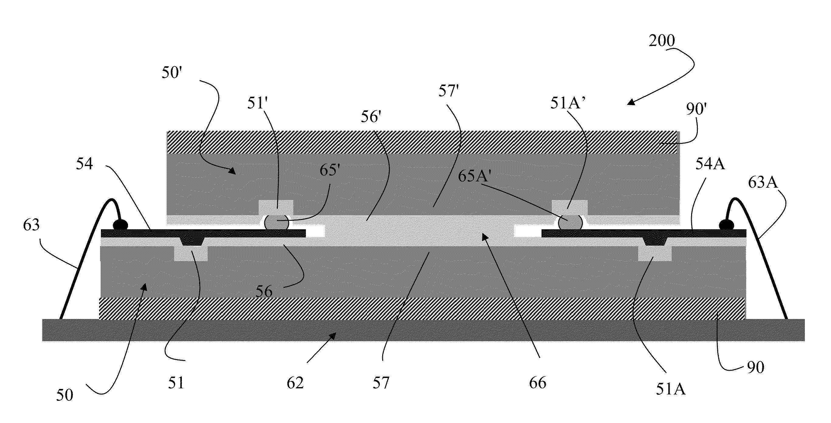
A method performs electrical testing and assembly of an electronic device on a wafer and comprising a pad made in an oxide layer covered by a passivation layer. The method includes connecting the electronic device to a testing apparatus; providing said electronic device with a metallization layer extending on the passivation layer from the pad to a non-active area of said wafer. The method comprises-performing the electrical testing on wafer of the electronic device by placing a probe of on a portion of the extended metallization layer; performing the cut of said wafer, reducing the extension of the metallization layer to the edge of the electronic device; embedding the device inside a package, forming on the metallization layer an electrical connection configured to connect the metallization layer to a circuit in said package.

Description

BACKGROUND[0001]1. Technical Field[0002]The present disclosure relates to a method to perform electrical testing and assembly of electronic devices.[0003]The present disclosure also relates to an electronic device comprised in a wafer comprising at least one pad made in an oxide layer covered by a passivation layer and subjected to electrical testing.[0004]The present disclosure also relates to a multichip system in package.[0005]The disclosure particularly, but not exclusively, relates to a method to perform an electrical testing and the assembly of electronic devices, of the type comprising for example a testing on wafer of the “Electrical Wafer Sort” (EWS) type or of the “Final Test” type or, again, testing of embedded devices “System in Package” (SiP), or, again, testing of the “Wafer Level Burn-In” (WLBI) type.[0006]2. Description of the Related Art[0007]As it is well known, one can perform an electrical testing on wafer of the EWS type, by electrically connecting a testing app...

Claims


Application Information

Patent Timeline
Patent Type & Authority Applications(United States)
IPC IPC(8): H01L21/66
CPCH01L22/32H01L2224/05553H01L24/32H01L24/48H01L24/49H01L24/73H01L25/0652H01L25/0657H01L2224/13025H01L2224/16145H01L2224/32145H01L2224/48091H01L2224/48145H01L2224/48147H01L2224/48227H01L2224/48464H01L2224/49109H01L2224/73207H01L2225/06506H01L2225/0651H01L2225/06513H01L2225/06517H01L2225/06541H01L2924/01014H01L2924/01029H01L2924/01033H01L2924/14H01L2924/30107H01L23/481H01L2924/1461H01L2224/0401H01L2224/05554H01L2224/48465H01L22/14H01L2924/01075H01L2924/01074H01L2924/01019H01L2924/01005H01L2924/00014H01L2924/00H01L2224/451H01L2224/05599H01L2224/85399G01R31/2818G01R31/2884H01L2224/04042H01L2224/04073H01L2224/16227H01L2224/17181H01L2224/73203H01L2224/73253H01L2224/73265H01L2224/023H01L2924/00015H01L2224/45015H01L2924/207H01L2224/45099H01L2924/0001
Inventor PAGANI, ALBERTO
Owner STMICROELECTRONICS SRL
Learn More