
Electrical connector insulator housing

a technology of insulator housing and connector, which is applied in the direction of electrical apparatus construction details, fixed connections, coupling device connections, etc., can solve the problems of housings that cannot be molded and/or can be difficult or impossible to replicate by machining, and cannot be molded or molded

Active Publication Date: 2013-03-28
HSIO TECH
View PDF6 Cites 62 Cited by
  • Summary
  • Abstract
  • Description
  • Claims
  • Application Information

AI Technical Summary

Benefits of technology

The present patent is about a new insulator socket housing that combines the benefits of traditional molded or machined socket housings with the flexibility of additive printing technology. This new housing can be digitally produced without tooling or costly artwork, with significant reductions in environmental issues. It can be used with a variety of contact members or interconnect types, and can be positioned at different locations, heights, or spacing. The housing can be manufactured in layers, with the ability to add metal materials to create electrical paths or improve performance. The new housing can also serve as a platform to add passive and active circuit features to improve electrical performance or internal function and intelligence. The conductive traces and grounding schemes can reduce the number of connections to the PCB and improve performance. Overall, the new housing has improved electrical performance and reduced complexity.

Problems solved by technology

The nature of the construction enables features and structures that cannot be molded and / or can be difficult to replicate by machining, such as for example, undercuts and hollows.
Considering the structure as an aggregate of dielectrics also allows for multiple materials to be used within one housing which is difficult or impossible with molding or machining.

Method used


Image

  • Electrical connector insulator housing
  • Electrical connector insulator housing
  • Electrical connector insulator housing

Examples


Embodiment Construction

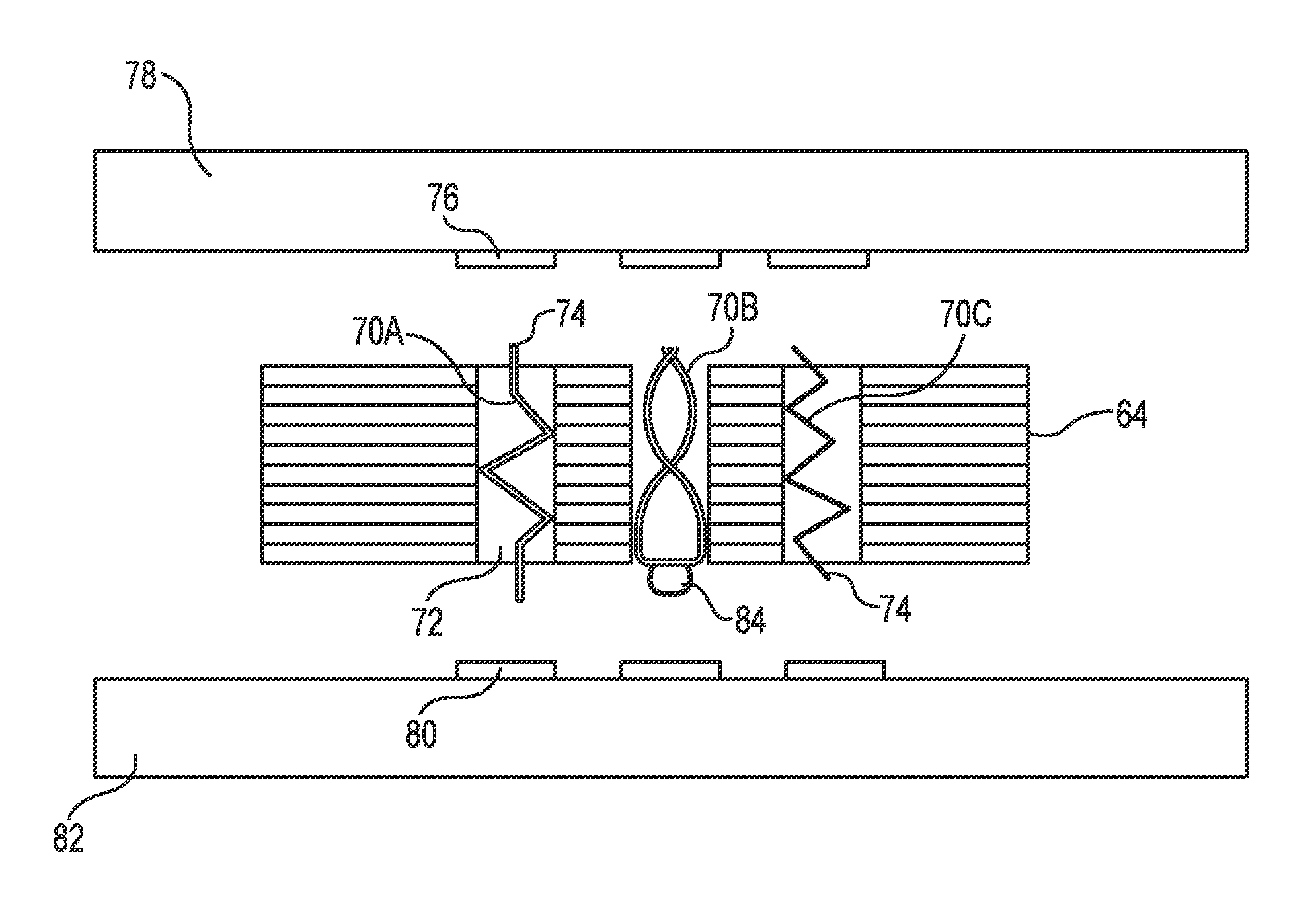
[0029]An insulator socket housing according to the present disclosure may permit fine contact-to-contact spacing (pitch) on the order of less than 1.0 mm pitch, and more preferably a pitch of less than about 0.7 millimeter, and most preferably a pitch of less than about 0.4 millimeter. Such fine pitch socket housings are especially useful for communications, wireless, and memory devices.

[0030]The present insulator socket housing can be configured as a low cost, high signal performance interconnect assembly, which has a low profile that is particularly useful for desktop and mobile PC applications. IC devices can be installed and uninstalled without the need to reflow solder. The solder-free electrical connection of the IC devices is environmentally friendly.

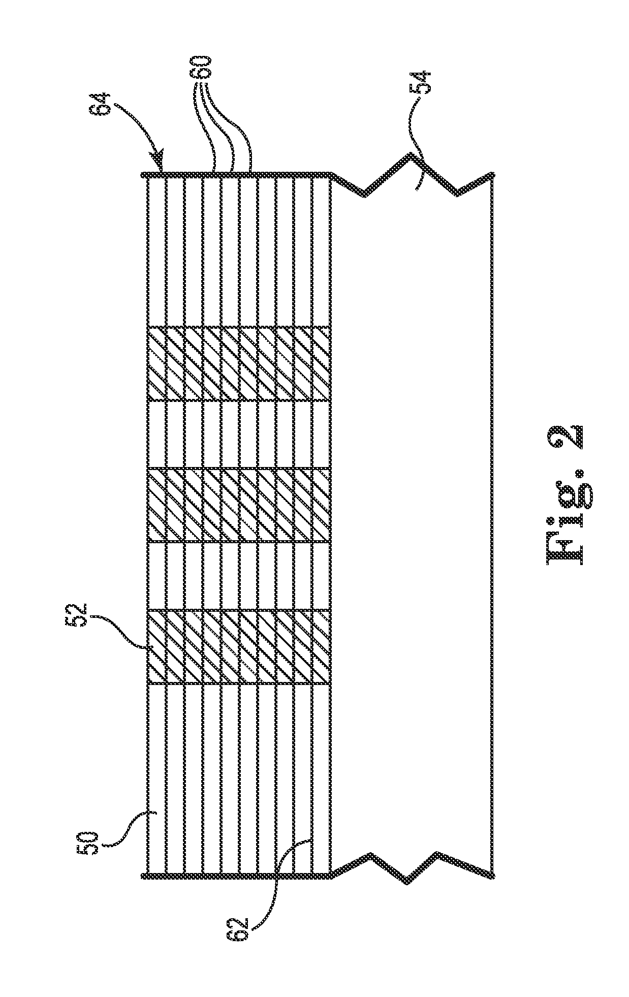
[0031]FIG. 1 is a side cross-sectional view of a method for replicating a socket housing using additive processes in accordance with an embodiment of the present disclosure. Dielectric layer 50 and removable or dissolvable materi...


PUM

PropertyMeasurementUnit
aspect ratioaaaaaaaaaa
widthaaaaaaaaaa

Abstract

A socket housing and method of making the socket housing. A plurality of dielectric layers are printed with a plurality of recesses on a substrate. The dielectric layers include at least two different dielectric materials. A sacrificial material is printed ted in the recesses. The assembly is removed from the substrate and the sacrificial material is removed from the recesses. At least one contact member is located in a plurality of the recesses. Distal ends of the contact members are adapted to electrically couple with circuit members.

Description

TECHNICAL FIELD[0001]The present application relates to an insulator connector socket housing that merges the long-term performance advantages of traditional socket manufacturing techniques with the flexibility of additive printing technology.BACKGROUND OF THE INVENTION[0002]Connectors and socket housings are typically manufactured by injection molding precision grade polymers, such as ABS, LCP. For smaller volume applications the connectors and socket housings are often precision machined from a dielectric material. Metallic contacts are inserted into the socket housing and retained by some sort of mechanical interference or captured such that they do not fall out during use. In some cases, the contacts are inserted into the mold prior to injection such that the polymer material flows around portions of the contacts.[0003]In both cases, the base material is typically loaded with glass fibers or particles to provide strength and mechanical or dimensional stability. In situations whe...

Claims


Application Information

Patent Timeline
Patent Type & Authority Applications(United States)
IPC IPC(8): H01R13/24H01R43/20H01R13/66
CPCH01R12/52H01R12/7082H01R13/2421H05K3/361H05K3/368Y10T29/4922H05K2201/0187H05K2201/10378H01R13/24H01R13/66H01R43/20H05K7/1069
Inventor RATHBURN, JAMES
Owner HSIO TECH
Learn More