
Large area hermetic encapsulation of an optoelectronic device using vacuum lamination

a technology of optoelectronic devices and vacuum lamination, which is applied in the manufacture of final products, sustainable manufacturing/processing, other domestic articles, etc., can solve the problems of reducing performance and aesthetically dissatisfactory products, and achieves short cycle times, reduce or prevent damage or stress of the front sheet, and minimize gas entrapment

Active Publication Date: 2013-03-21
BOE TECH GRP CO LTD
View PDF18 Cites 6 Cited by
  • Summary
  • Abstract
  • Description
  • Claims
  • Application Information

AI Technical Summary

Benefits of technology

The present invention is related to a vacuum laminator and lamination techniques for producing large area hermetically encapsulated optoelectronic devices with short cycle times. The laminator is designed to minimize damage or stress of the front sheet, prevent gas-bubble entrapment, and achieve accurate placement and fill-factor optimization. The technical effects of the invention include reducing manufacturing defects and improving shelf life characteristics of the products, as well as optimizing the placement head, controlling pressure balance, and utilizing cooling passages and platen heaters for efficient cooling and heating of the platen.

Problems solved by technology

This, along with the placement operation being performed under vacuum, eliminates gas-bubble entrapment which can create a decrease in performance and aesthetically dissatisfying products.

Method used

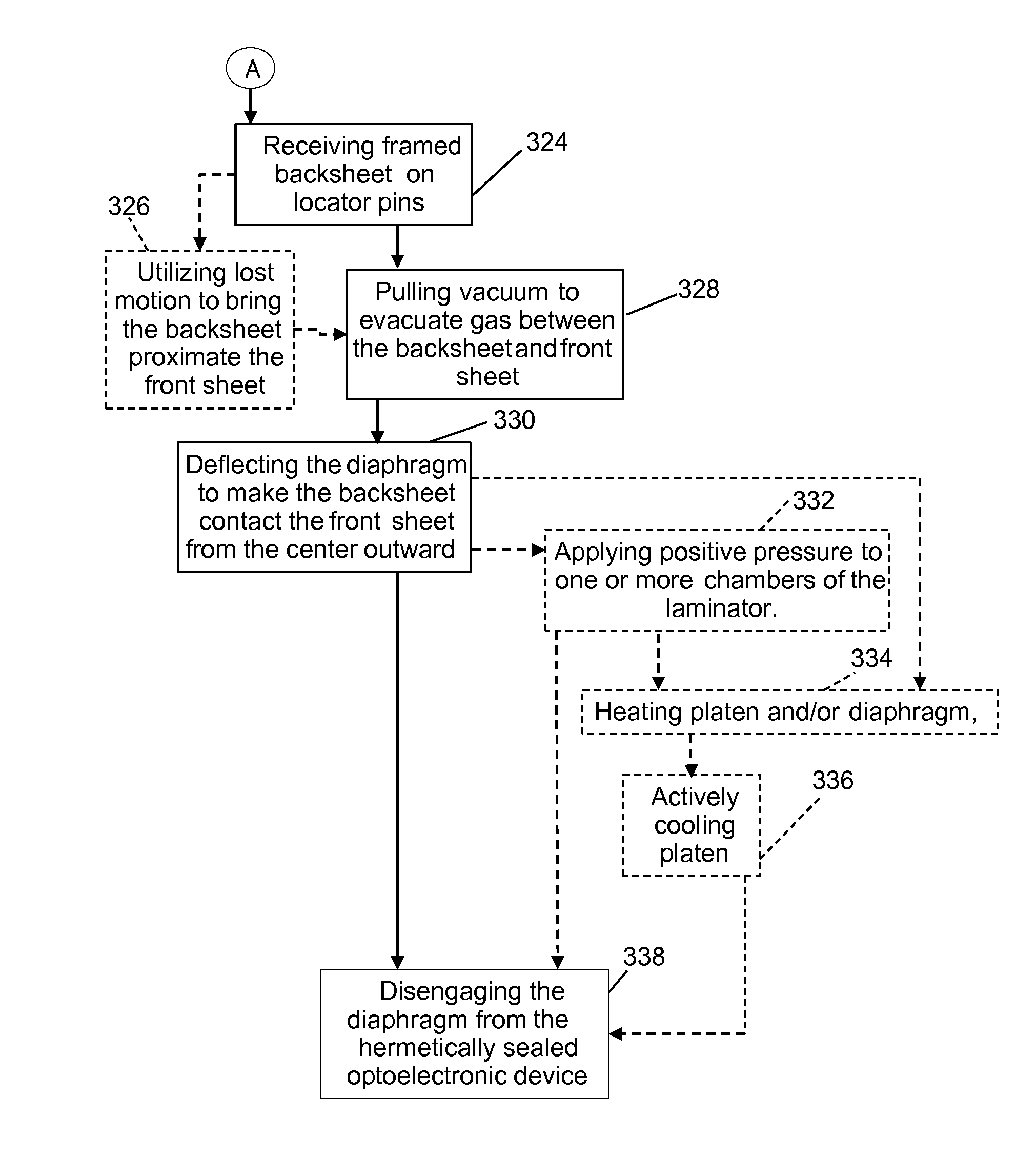

Image

  • Large area hermetic encapsulation of an optoelectronic device using vacuum lamination
  • Large area hermetic encapsulation of an optoelectronic device using vacuum lamination
  • Large area hermetic encapsulation of an optoelectronic device using vacuum lamination

Examples


Embodiment Construction

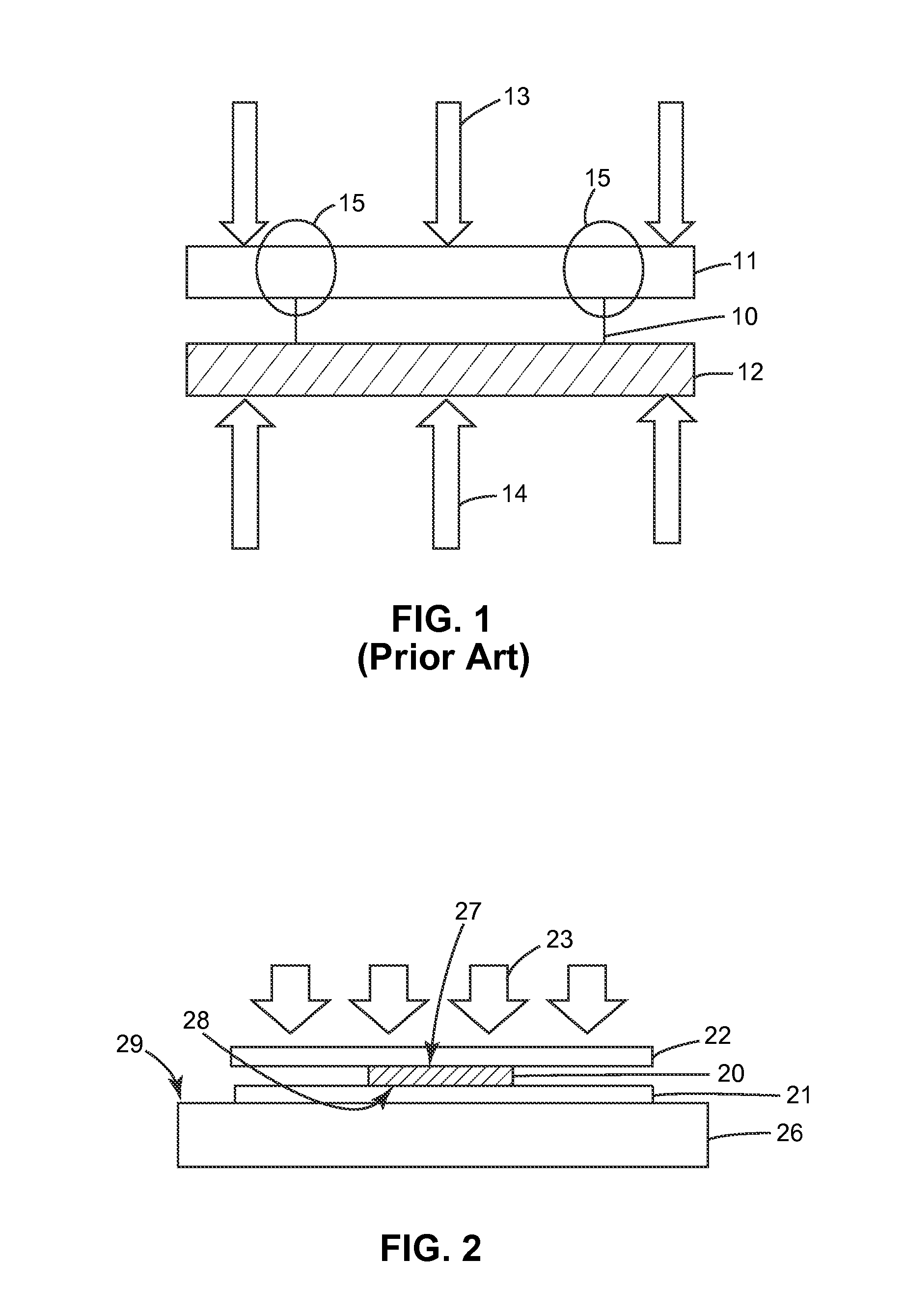
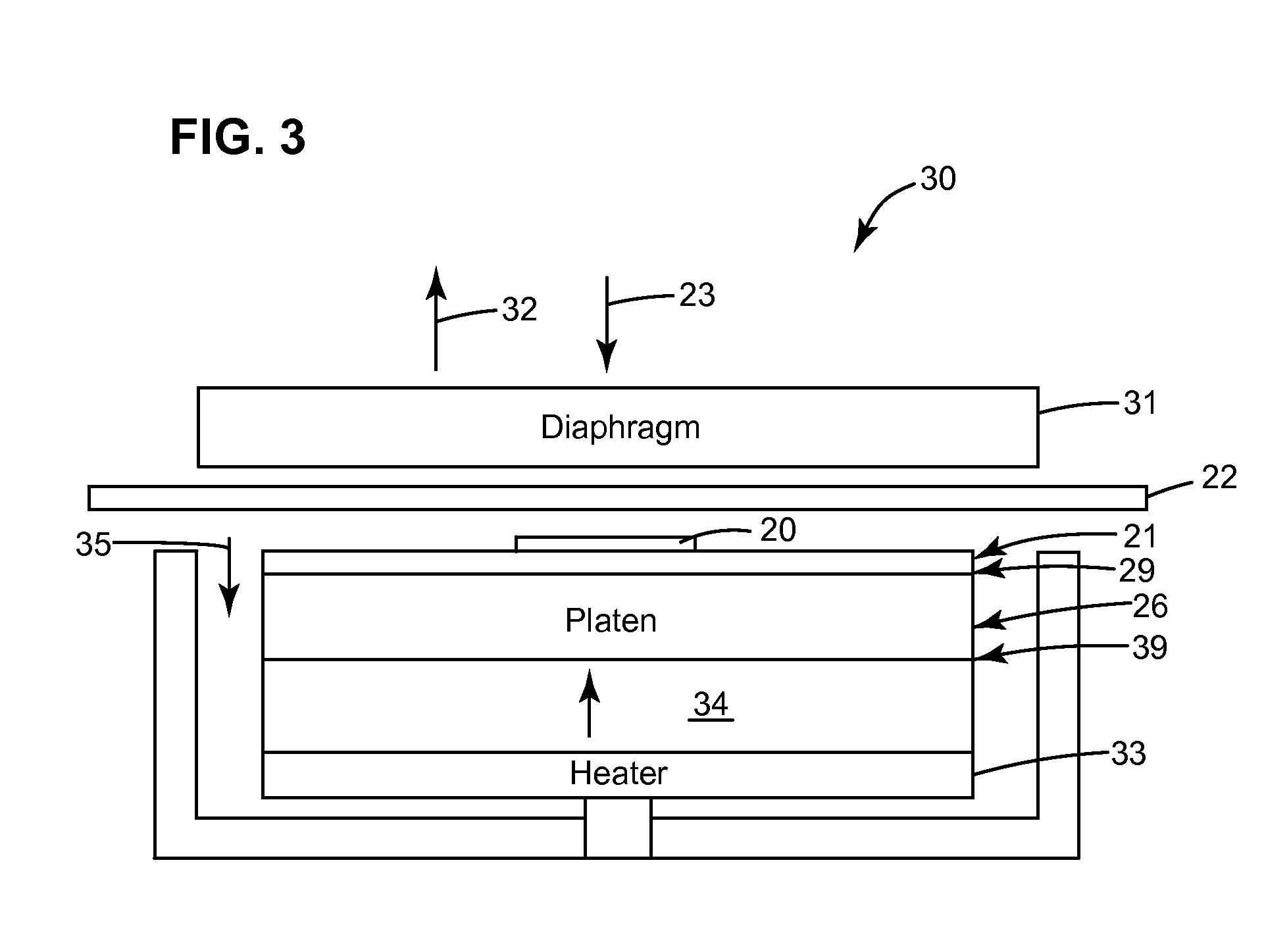
[0037]FIG. 2 is a diagram illustrating compressive forces 23 applied to a backsheet 22 of an optoelectronic device 20, such as an OLED device or a photovoltaic device, by an embodiment of a new vacuum laminator (30 in FIG. 3). The optoelectronic device 20 is positioned between the backsheet 22 and a front sheet 21. The front sheet 21 may comprise an ultra-high barrier (UHB) film, an optical coupler, an out-coupling adhesive, and / or an out-coupling film. The backsheet 22 contacts a first surface 27 of the optoelectronic device 20. The front sheet 21 contacts an opposite surface 28 of the optoelectronic device 20 and is positioned on a fiat surface 29 of a platen 26.

[0038]Accordingly, in contrast to conventional roll lamination techniques, the front sheet 21 remains flat, and only the backsheet 22 is pressured to conform around the perimeter of the optoelectronic device 20. Therefore, the mechanically sensitive front sheet 21 is not subjected to the high stress concentrators that are ...


PUM

PropertyMeasurementUnit
Forceaaaaaaaaaa
Pressureaaaaaaaaaa
Shapeaaaaaaaaaa

Abstract

Apparatus for accurately picking and placing one or more optoelectronic devices for vacuum lamination of materials in a way that minimizes stress to the materials.

Description

BACKGROUND OF THE INVENTION[0001]1. Field of the Invention[0002]The field of the invention relates to optoelectronic devices generally, and more particularly to certain new and useful advances in the manufacture of encapsulated optoelectronic devices.[0003]2. Description of Related Art[0004]Optoelectronic devices generally comprise light emitting devices and photovoltaic devices. Both types of optoelectronic devices comprise an active layer sandwiched between two electrodes, at least one of which is usually transparent in a light emitting device, a voltage applied between the two electrodes generates electrical current through the active layer, which causes the active layer to emit light. In a photovoltaic device, such as a solar cell, the active layer absorbs energy from light and converts this absorbed energy to electrical energy, which is evidenced as a voltage and / or a current between the two electrodes.[0005]The active layer is either an inorganic or organic electroluminescent ...

Claims


Application Information

Patent Timeline
IPC IPC(8): H01L33/52B32B37/00H01L31/18B32B38/18
CPCB32B37/003B32B37/1018H01L51/448H01L51/524Y10T156/17B32B2457/12B32B2457/206Y02E10/549H01L31/048Y02P70/50H10K30/88H10K50/841
Inventor KOSTKA, JAMES MICHAELBALASCHAK, EDWARD JAMESKNAPP, THOMAS ALEXANDERCHARNY, JOHN ALLIE
Owner BOE TECH GRP CO LTD
Learn More