Eureka AIR delivers breakthrough ideas for toughest innovation challenges, trusted by R&D personnel around the world.

Planar srfet using no additional masks and layout method

a technology of srfet and layout method, applied in semiconductor devices, diodes, electrical apparatus, etc., can solve the problems of increasing manufacturing costs, more complicated processes, and increasing manufacturing costs, and achieve the effect of preventing an early breakdown, enhancing the performance of schottky diodes, and maximizing the schottky area

Active Publication Date: 2013-01-31
ALPHA & OMEGA SEMICON INC
View PDF3 Cites 39 Cited by
  • Summary
  • Abstract
  • Description
  • Claims
  • Application Information

AI Technical Summary

Benefits of technology

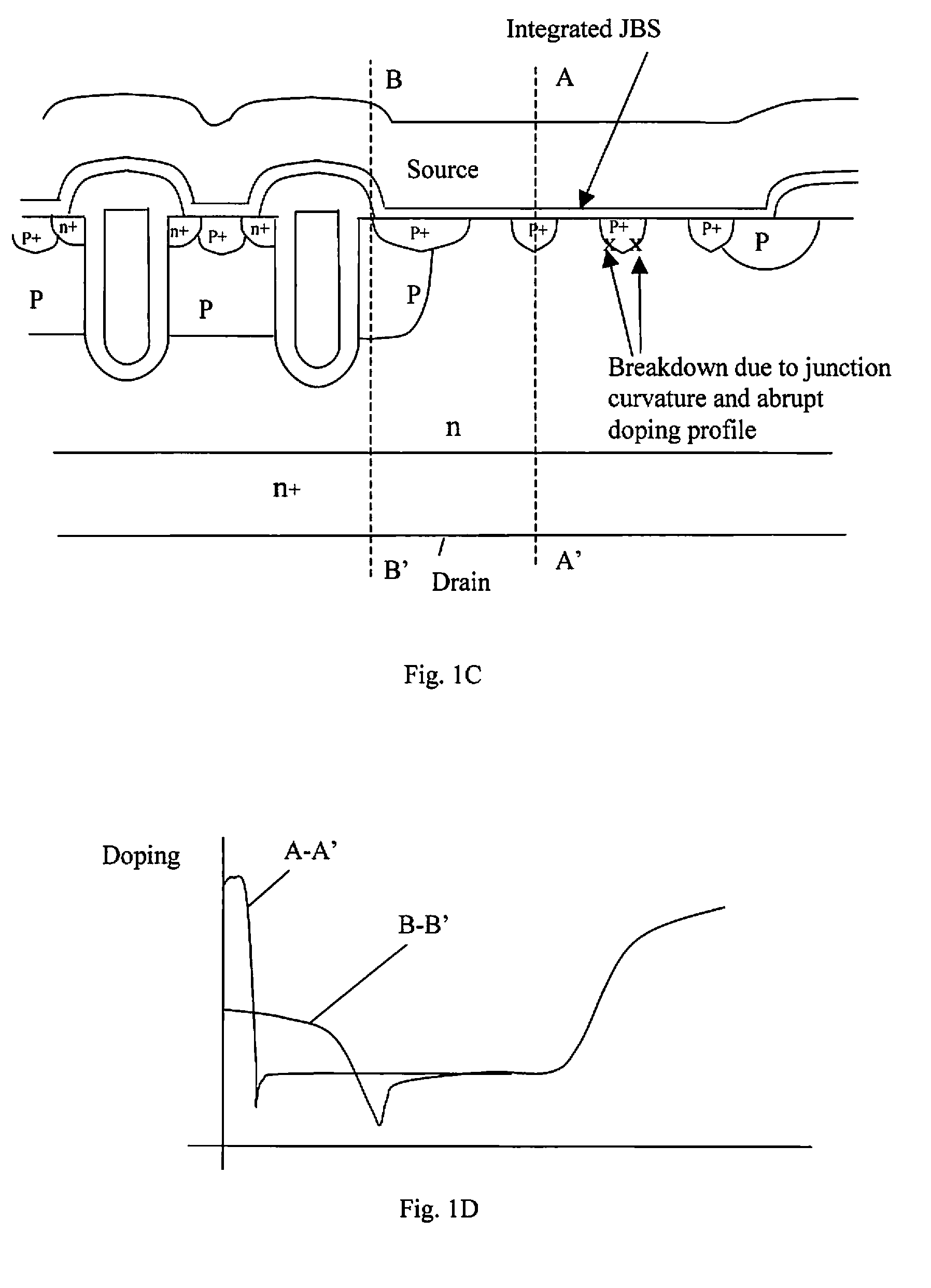
The present invention provides new and improved manufacturing processes and device configuration for the planar MOSFET integrated with Schottky diodes. These processes and configurations are implemented without requiring additional masks, resulting in reduced production costs. The invention also provides new layout configurations of the MOSFET device integrated with Schottky diodes with higher cell density and improved device performances. Additionally, the invention improves the breakdown voltage of the device and increases the doping concentration in the Schottky diordinates to enhance its performance. Overall, the invention provides better efficiency, reliability, and performance of semiconductor power devices with Schottky diodes.

Problems solved by technology

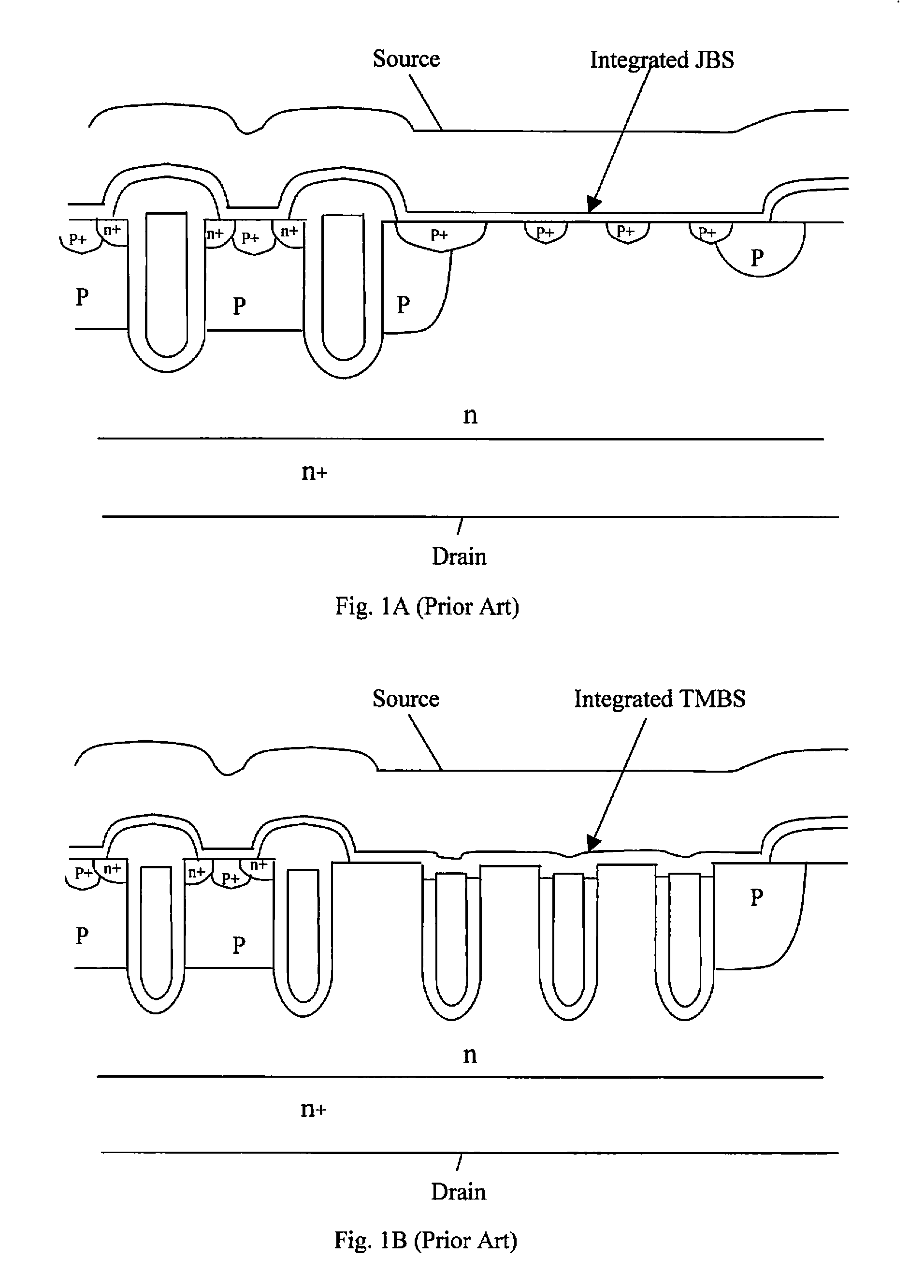
However, conventional ways of manufacturing the planar MOSFET devices with integrated Schottky diodes often require additional masks for the formation of the Schottky diodes in an Schottky regions between the MOSFET cells.
Therefore, higher manufacturing costs and more complicate processes are necessary for implementing the planar MOSFET device with the Schottky diodes.
However, there is a tradeoff that due to an increase of the series resistance.
However, these devices still have the limitations of using metals of relatively high barrier height.
The device performance cannot satisfy the modern applications that require further reduction on resistance and higher drive currents.
However, the high barrier height metal as required to achieve acceptable low leakage current in the off state presents a disadvantage due to the higher costs of depositing both the high barrier height metal and the low barrier height metal to meet the requirements of Schottky and source-body ohmic contact.

Method used


Image

  • Planar srfet using no additional masks and layout method
  • Planar srfet using no additional masks and layout method
  • Planar srfet using no additional masks and layout method

Examples


Embodiment Construction

[0040]Referring to FIGS. 3A and 3B for the side cross sectional views of the JBS area to provide the rectification function for a MOSFET device. FIG. 3A shows a blank implant of a low dose of body type dopant ions. For N channel MOSFET device, Boron ions with dosage 5×10¹¹ to 5×10¹² / cm2 may be implanted into the epitaxial layer with energy from 40-500 Kev, preferably with 80-300 Kev. The blank implant of the body type dopant ions is to compensate and lower the doping concentration of a portion of the epitaxial layer to increase epitaxial layer breakdown voltage. In FIG. 3B, the body dopant is then diffused by applying an elevated diffusion temperature ranging from 1000 to 1150 degrees for 1 to 3 hours to diffusion the body type dopant into a depth shallower than the depth of MOSFET body region form in a later step. The implanting body type dopant ions compensate a portion of epi dopant and generate an N− region in the epitaxial layer. This would not significantly affect the MOSFET b...


PUM


Abstract

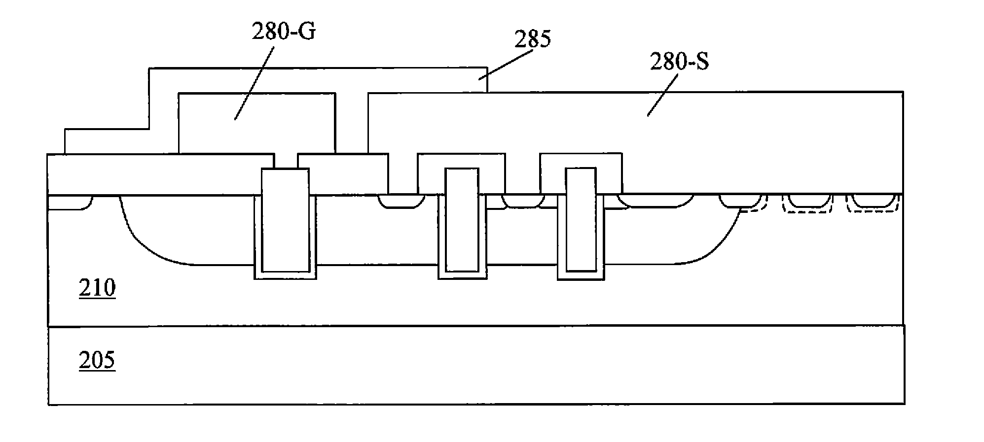
A semiconductor power device is supported on a semiconductor substrate with a bottom layer functioning as a bottom electrode and an epitaxial layer overlying the bottom layer as the bottom layer. The semiconductor power device includes a plurality of FET cells and each cell further includes a body region extending from a top surface into the epitaxial layer. The body region encompasses a heavy body dopant region. An insulated gate is disposed on the top surface of the epitaxial layer, overlapping a first portion of the body region. A barrier control layer is disposed on the top surface of the epitaxial layer next to the body region away from the insulated gate. A conductive layer overlies the top surface of the epitaxial layer covering a second portion of the body region and the heavy body dopant region extending over the barrier control layer forming a Schottky junction diode.

Description

[0001]This Patent Application is a Divisional Application and claims the Priority Date of a co-pending application Ser. No. 11 / 906,746 filed by common inventors of this Application on Oct. 1, 2007. Aplication Ser. No. 11 / 906,746 is a Continuation in Part (CIP) Application of two co-pending Applications with a Ser. Nos. 11 / 056,346 and 11 / 413,249 filed by a common Inventor of this Application on Feb. 11, 2005 and Apr. 29, 2006 and now issued into U.S. Pat. Nos. 7,285,822 and 7,436,022 respectively. The Disclosures made in these applications Ser. Nos. 11 / 056,346, 11 / 413,249, and 11 / 906,746 are hereby incorporated by reference.BACKGROUND OF THE INVENTION[0002]1. Field of the Invention[0003]The invention relates generally to the semiconductor power devices. More particularly, this invention relates to an improved and novel manufacturing process and device configuration for integrating an MPS (Merged P-i-N / Schottky) Schottky into a planar MOSFET that does not require additional masks whil...

Claims


Application Information

Patent Timeline
Patent Type & Authority Applications(United States)
IPC IPC(8): H01L27/088H01L21/336
CPCH01L29/4236H01L29/456H01L29/47H01L29/66712H01L29/66734H01L29/7806H01L29/872H01L29/7813H01L29/0619H01L29/0696H01L29/0878H01L29/1095H01L29/7811H01L29/8725
Inventor BHALLA, ANUP
Owner ALPHA & OMEGA SEMICON INC
Why Eureka
Eureka Blog
Learn More