Inverter

a technology of inverter and gate drive circuit, which is applied in the field of inverter, can solve the problems of complex structure of gate drive circuit, and achieve the effect of reducing switching losses and speeding up switching speed

Inactive Publication Date: 2013-01-24
PANASONIC CORP
View PDF3 Cites 16 Cited by
  • Summary
  • Abstract
  • Description
  • Claims
  • Application Information

AI Technical Summary

Benefits of technology

The present invention is about an inverter that can reduce switching losses and improve efficiency. The inverter includes switches that have both forward and reverse conductivity, allowing for synchronous rectification. The switches also have a diode region that is only conductive in the reverse direction, acting as freewheeling diodes. The inverter can operate without a short circuit current flow when the switches are in the on-state for a predetermined time period. The gate drive circuit controls the switches to synchronize their timing, without requiring a structure for generating gate drive signals with dead times. The use of unipolar diodes prevents the flow of a short circuit current even if there are time periods in which both switches are in the off-state. Overall, the invention improves the performance and efficiency of the inverter.

Problems solved by technology

This gives rise to the problem that the structure of the gate drive circuits is complicated.

Method used


Image

  • Inverter
  • Inverter
  • Inverter

Examples


first embodiment

[0055]

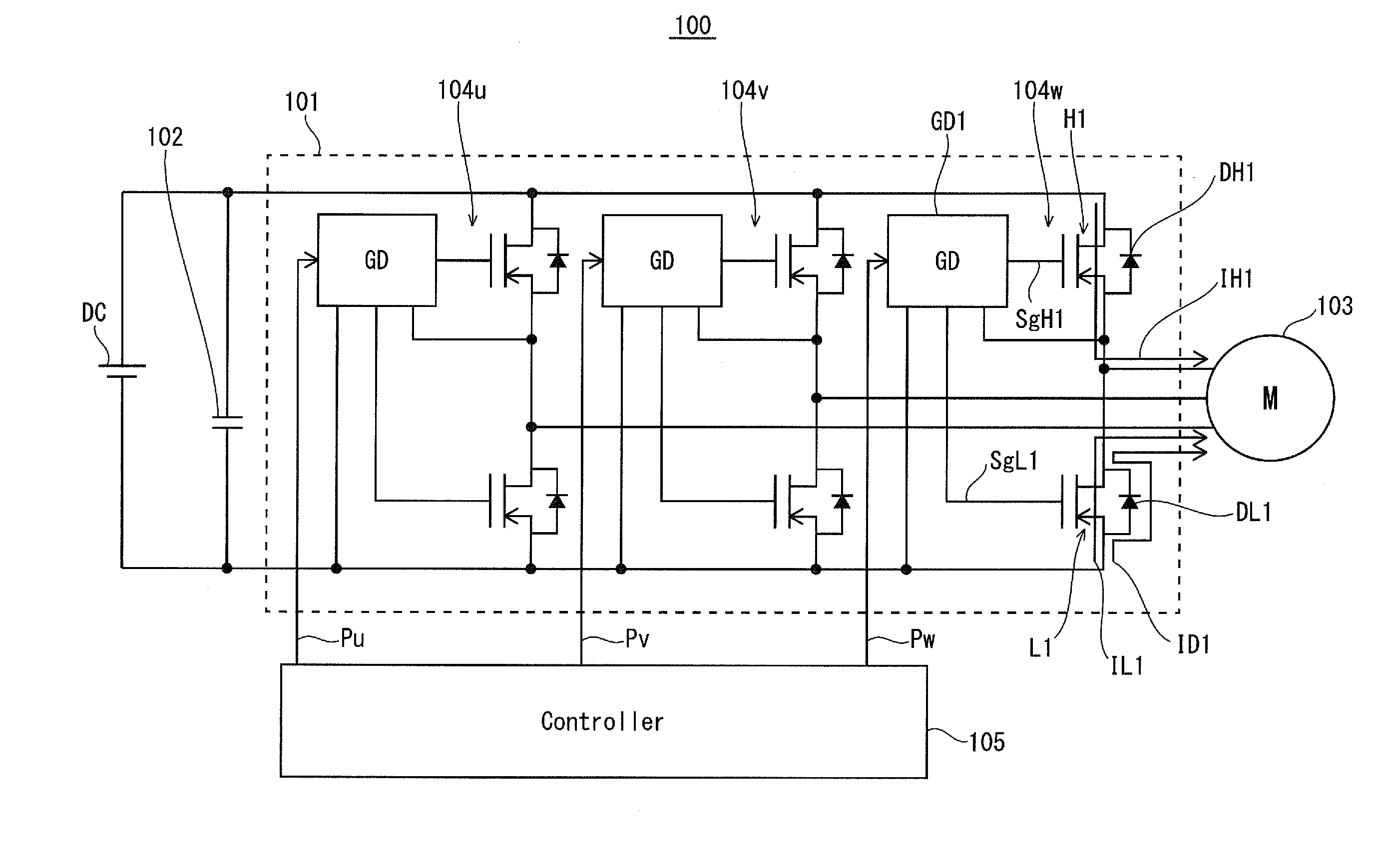
[0056]FIG. 1 shows an overall structure of a load driving system 100 including an inverter pertaining to First Embodiment. The present embodiment describes a structure in which a three-phase AC motor serves as the load.

[0057]The load driving system 100 includes a direct current power supply DC, an inverter 101, a smoothing capacitor 102, a three-phase AC motor 103, and a controller 105.

[0058]For example, the direct current power supply DC may obtain a direct current by rectifying a power supply system. Alternatively, the direct current power supply DC may be in the form of a battery (representative examples include secondary batteries such as a nickel-metal hydride battery and a lithium-ion battery).

[0059]The inverter 101 converts a direct current supplied from the direct current power supply DC into a three-phase alternating current, and supplies the three-phase alternating current to the three-phase AC motor 103. The three phases, namely a U phase, a V phase and a W phase, a...

second embodiment

[0131]The following describes Second Embodiment with a focus on differences from First Embodiment. Note that the timing chart pertaining to the present embodiment is similar to the timing chart of FIGS. 4A through 4I, and is therefore omitted from the following description.

[0132]

[0133]FIG. 9 shows an overall structure of a load driving system 200 including an inverter pertaining to Second Embodiment. The load driving system 200 differs from the load driving system 100 pertaining to First Embodiment in the structure of an inverter 201, especially in the structure of switches H2 and L2. Note that constituent elements of the load driving system 200 that are the same as those of the load driving system 100 have the same reference signs thereas, and are omitted from the following description.

[0134]As with the inverter 101 pertaining to First Embodiment, the inverter 201 includes a U-phase arm 204u, a V-phase arm 204v and a W-phase arm 204w. The W-phase arm 204w includes a high-side switc...

third embodiment

[0187]The present embodiment provides a description of a gate drive circuit structured such that a short circuit current is more difficult to flow between switches.

[0188]FIG. 23A shows a circuit structure of a gate drive circuit pertaining to the present embodiment. FIG. 23B shows fluctuations in a terminal-to-terminal voltage of each switch during the switching operation. Note that the reference signs of constituent elements shown in FIG. 23A are basically the same as the reference signs of constituent elements shown in FIG. 1. Although the following description relates only to the high-side switch, the same goes for the low-side switch.

[0189]A description is now given of the switching operation performed by the switch with reference to FIGS. 23A and 23B, with a focus on charge and discharge of a gate capacitance between the gate electrode and the source electrode of the switch (hereinafter, simply “a gate capacitance of the switch”).

[0190]As shown in FIG. 23B, in an interval X, th...


PUM


Abstract

An inverter comprising: a circuit including arms connected in parallel, each of the arms including a first switch and a second switch connected in series; and a gate drive circuit configured to control, by pulse-width modulation using synchronous rectification, each of the first switch and the second switch to switch to an on-state or an off-state, wherein each of the first switch and the second switch includes: a channel region that is conductive in both a forward direction and a reverse direction in the on-state, and that is not conductive in the forward direction in the off-state; and a diode region that is combined as one with the channel region, and that is conductive only in the reverse direction, the diode region being unipolar, and the gate drive circuit synchronizes a timing at which the gate drive circuit outputs a signal for causing the first switch to switch to the on-state with a timing at which the gate drive circuit outputs a signal for causing the second switch to switch to the off-state, and synchronizes a timing at which the gate drive circuit outputs a signal for causing the first switch to switch to the off-state with a timing at which the gate drive circuit outputs a signal for causing the second switch to switch to the on-state.

Description

TECHNICAL FIELD[0001]The present invention relates to technology for simplifying the structure of an inverter utilizing synchronous rectification, especially the structure of a gate drive circuit in the inverter.BACKGROUND ART[0002]There is a conventional inverter utilizing synchronous rectification, that is, an inverter that performs a rectification process by synchronizing the operation of a rectifier switch (rectifier element) with the operation of a main switch (for example, Patent Literature 1). Such an inverter utilizing synchronous rectification brings about the advantage that the power conversion efficiency can be improved by causing the rectifier switch to operate with a voltage lower than the on-voltage for a freewheeling diode. Note, the on-voltage for the freewheeling diode is a voltage required to turn on the freewheeling diode.[0003]FIG. 26 shows an overall structure of a load driving system that includes an inverter utilizing synchronous rectification.[0004]A load dri...

Claims


Application Information

Patent Timeline
IPC IPC(8): H02M7/538
CPCH02M7/5387H02M7/003H01L29/1608H01L29/7806H01L29/7828H01L29/66068
Inventor KITABATAKE, MAKOTOKAZAMA, SHUN
Owner PANASONIC CORP
Why Eureka
Try Eureka