Memory device with trimmable power gating capabilities

a memory device and power gating technology, applied in the field of memory devices, can solve the problems of both stability and leakage of the memory device, and achieve the effect of reducing the standby leakage current of the entire memory device and reducing the standby leakage curren

Inactive Publication Date: 2013-01-17
AVAGO TECH WIRELESS IP SINGAPORE PTE
View PDF3 Cites 18 Cited by
  • Summary
  • Abstract
  • Description
  • Claims
  • Application Information

AI Technical Summary

Benefits of technology

The present invention is about memory devices that can be power gated after they have been formed. This is achieved by using a power gating circuit that controls the potential of a memory cell's source terminals. The circuit can set the source potential low to ground when the memory block is in an operational mode, and set it high when it is in standby mode. By doing this, it reduces the standby leakage currents and the entire memory device's standby leakage. The invention allows for fine-tuning of the power gating for individual memory blocks, based on the application of trimming signals.

Problems solved by technology

Such process variations may impact both stability and leakage in the memory devices.

Method used


Image

  • Memory device with trimmable power gating capabilities
  • Memory device with trimmable power gating capabilities
  • Memory device with trimmable power gating capabilities

Examples


Embodiment Construction

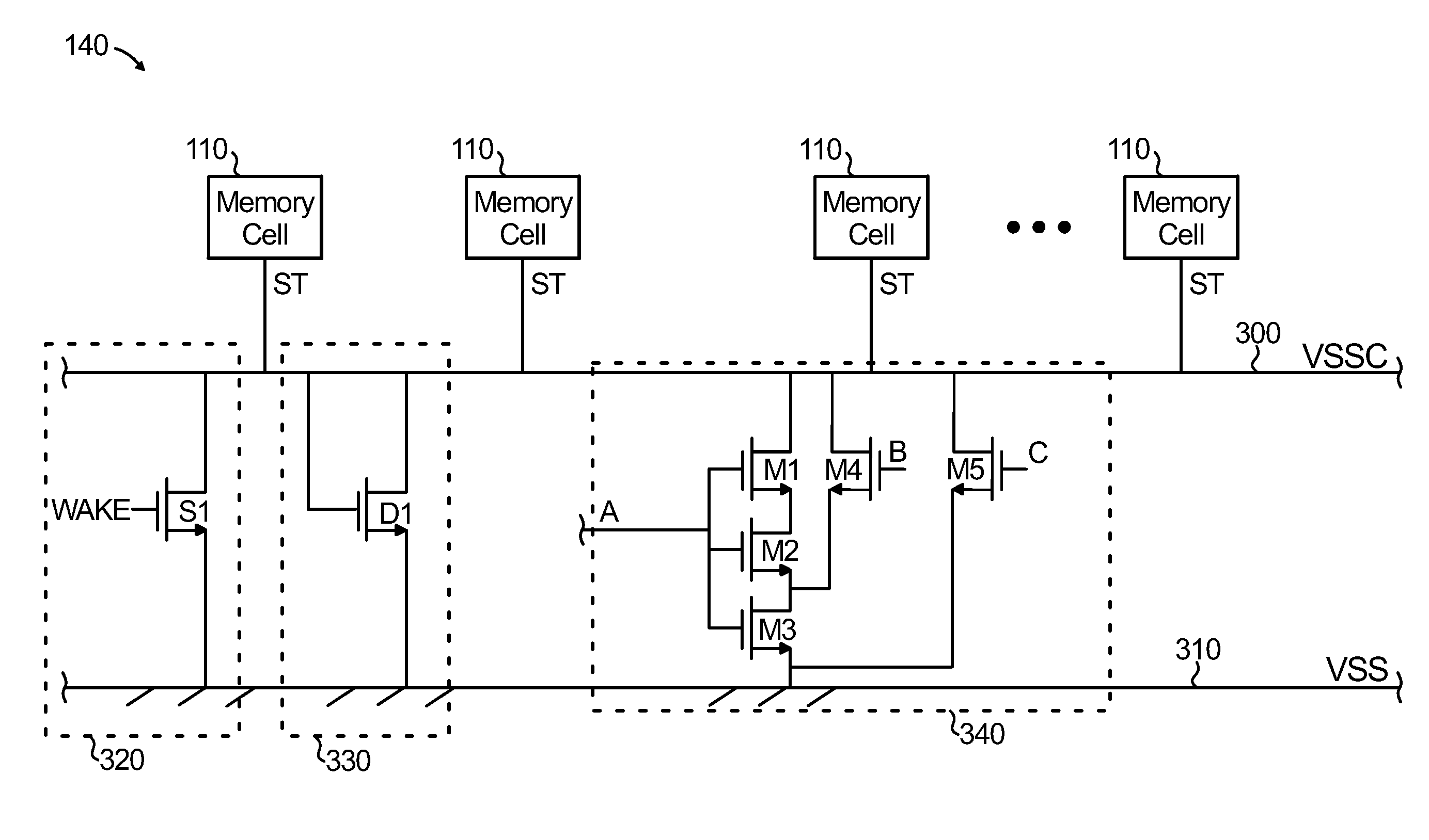
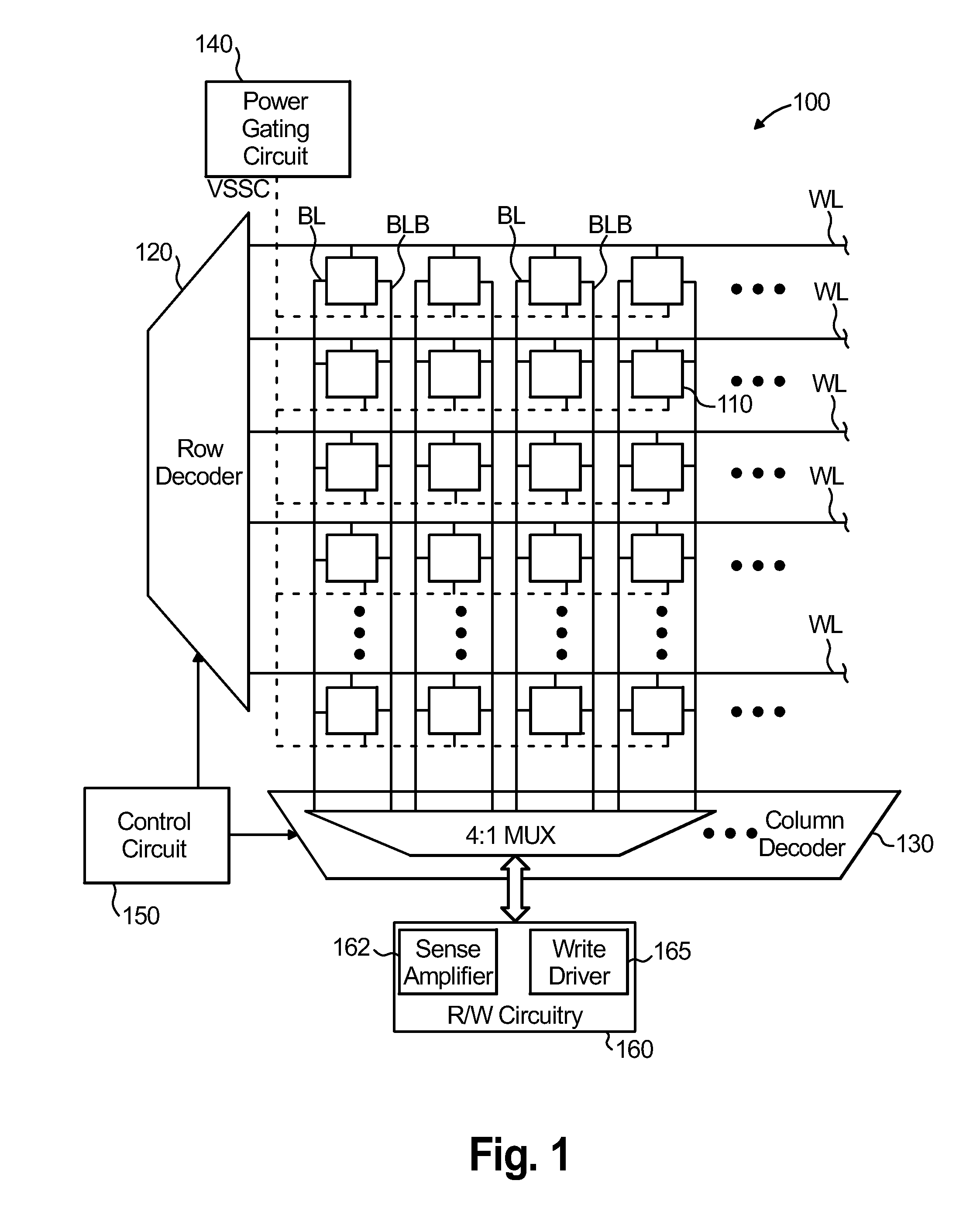
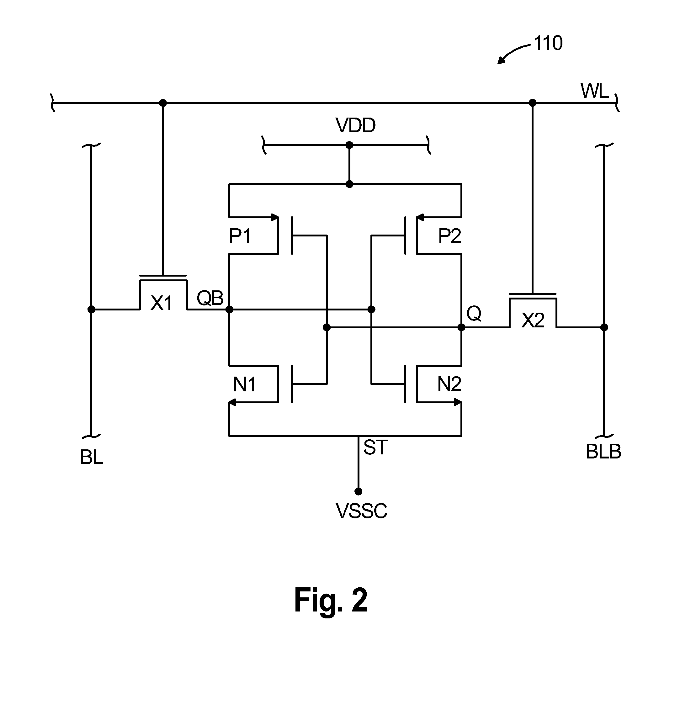
[0016]The present invention, according to aspects thereof, will be described herein in the context of illustrative memory devices having trimmable power gating circuitry. It should be understood, however, that the present invention is not limited to these or any other particular circuit arrangements. Rather, the invention is more generally applicable to techniques for improving standby leakage and stability in memory devices, among other advantages. Moreover, it will become apparent to those skilled in the art given the teachings herein that numerous modifications can be made to the embodiments shown that are within the scope of the present invention. That is, no limitations with respect to the specific embodiments described herein are intended or should be inferred.

[0017]For the purpose of describing and claiming the invention, the term MISFET as used herein is intended to be construed broadly and to encompass any type of metal-insulator-semiconductor field effect transistor. The t...


PUM


Abstract

A memory device includes at least one memory cell including a storage element electrically connected with a source potential line. A drive strength of the storage element is controlled as a function of a voltage level on the source potential line. The memory device further includes a clamp circuit electrically connected between the source potential line and a voltage source. The clamp circuit is operative to regulate the voltage level on the source potential line relative to the voltage source. A control circuit of the memory device is connected with the source potential line. The control circuit is operative to adjust the voltage level on the source potential line as a function of an operational mode of the memory device. A coarseness by which the voltage level on the source potential line is adjusted is selectively controlled as a function of at least a first control signal.

Description

FIELD OF THE INVENTION[0001]The present invention relates generally to electronic circuits, and, more particularly, to memory devices.BACKGROUND OF THE INVENTION[0002]As the feature sizes of metal-insulator-semiconductor (MIS) devices continue to shrink, the die-to-die and within-die variations in device parameters are continuously increasing. Process variations are particularly critical in semiconductor memory devices, where minimum geometry transistors are commonly utilized in order to conform to rigorous area constraints. Such process variations may impact both stability and leakage in the memory devices. For example, the static noise margin (SNM) of a static random access memory (SRAM) cell quantifies how much voltage noise is required at the cell's internal nodes to flip the cell's logic state. Previous results suggest that there may be almost a 30% variation in SNM with only a 10% variation in the threshold voltages and channel lengths of the transistors forming the SRAM.[0003...

Claims


Application Information

Patent Timeline
Patent Type & Authority Applications(United States)
IPC IPC(8): G11C7/00
CPCG11C7/02G11C11/417G11C5/147
Inventor GOEL, ANKURKONUDULA, VENKATESWARA REDDYGOWDA, SATHISHA NANJUNDE
Owner AVAGO TECH WIRELESS IP SINGAPORE PTE
Why Eureka
Try Eureka