Dram cell having buried bit line and manufacturing method thereof

a manufacturing method and buried bit technology, applied in the direction of semiconductor devices, electrical apparatus, transistors, etc., can solve the problems of reducing device reliability, affecting device performance, and traversing electric fields, so as to improve device performance, reduce device size, and optimize manufacturing methods

Inactive Publication Date: 2012-12-13
INOTERA MEMORIES INC
View PDF11 Cites 2 Cited by
  • Summary
  • Abstract
  • Description
  • Claims
  • Application Information

AI Technical Summary

Benefits of technology

[0007]One object of the instant disclosure is providing a dram cell having buried bit line and a manufacturing method thereof. The dram cell has buried bit line formed inside the substra...

Problems solved by technology

Thus, hot carrier effect may cause effluence to the device performance.
Contrary to the reduced device size, the operation voltage is still high to result in a traverse electric filed.
For example, when the channel of the transistor is less than 2 um, the reliability of the device may be decreased due to the hot carrier effect.
However,...

Method used


Image

  • Dram cell having buried bit line and manufacturing method thereof
  • Dram cell having buried bit line and manufacturing method thereof
  • Dram cell having buried bit line and manufacturing method thereof

Examples


Embodiment Construction

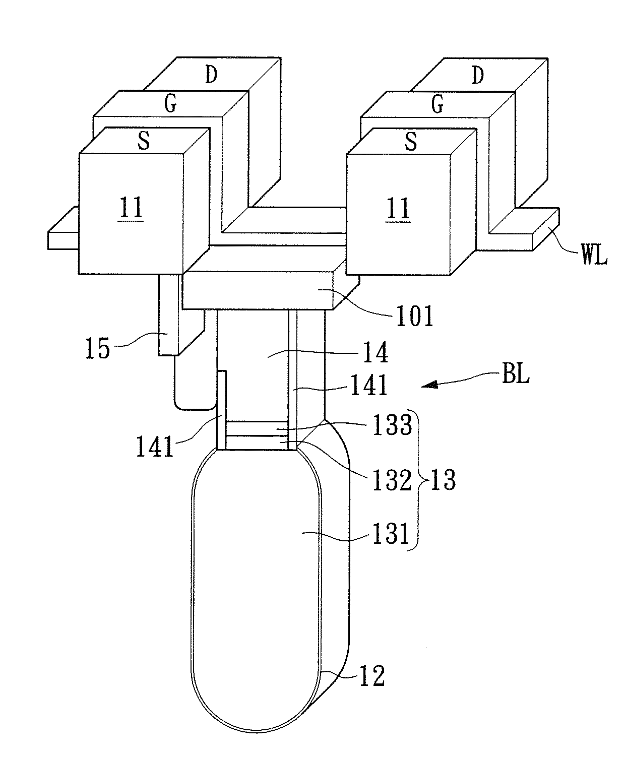
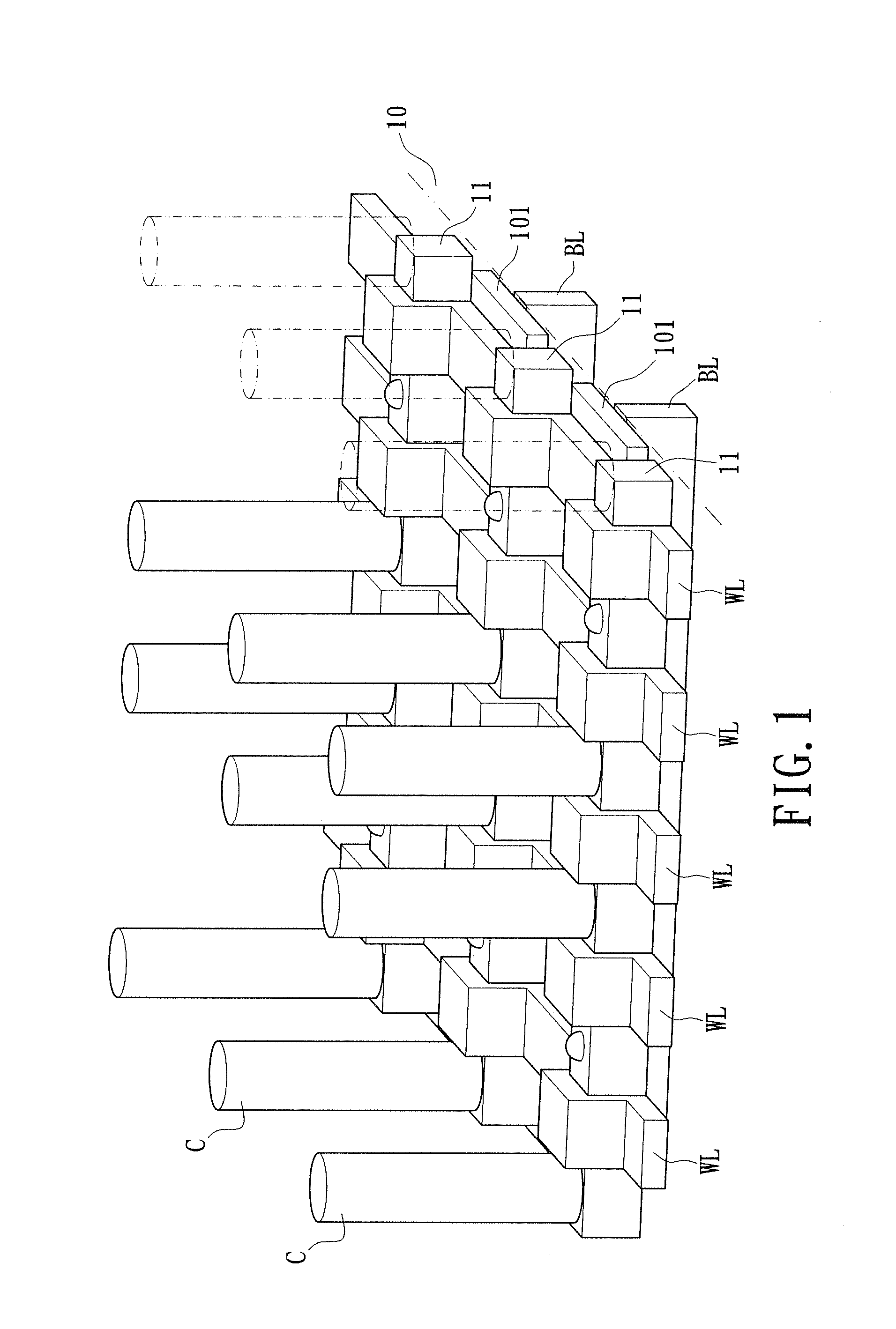
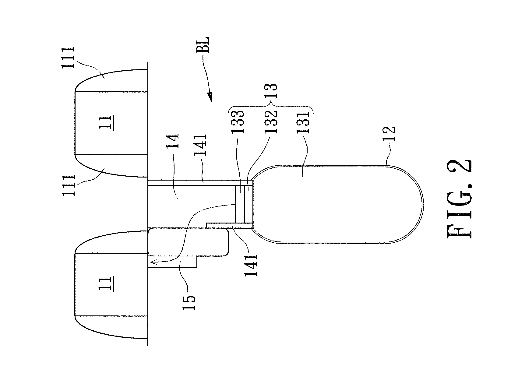
[0015]The present invention provides a dram (dynamic random access memory) cell having buried bit line and manufacturing method thereof. By using the double gate structure of the instant disclosure, the properties of the manufactured device are improved, especially for drain induction barrier lower effect (DIBL) of FET or sub-threshold swing. Therefore, the size of the dram cell may be reduced. Furthermore, because of the buried bit lines, the word lines, bit lines and active areas are substantially located on the same surface, the surface is more planar for performing processes thereon. For example, the planar surface is suitable for the manufacturing procedure of the double gate.

[0016]Please refer to FIGS. 1 to 3; the manufacturing method of the instant disclosure at least has the following steps.

[0017]Step 1 is providing a substrate 10 which has a plurality of fin structures 11 thereon. In the exemplary embodiment, a Si substrate is etched or produced in similar methods to form t...


PUM


Abstract

A dram cell having buried bit line includes a substrate having fin structures thereon, a plurality of deep trenches in the substrate, a buried stripe, a plurality of word lines formed on the substrate and a plurality of capacitors formed on the fin structures. Each of the deep trenches is arranged between two adjacent fin structures. Each of the deep trenches has a metal layer and a poly-silicon layer thereinside to define a buried bit line. The buried stripe is formed in the substrate and next to each of the deep trenches. The bit line is electrically connected to the corresponding fin structure via the buried stripe. The word lines are alternatively arranged with the bit lines, and each of the word lines are disposed cross on the fin structures to construct double gate structures.

Description

BACKGROUND OF THE INVENTION[0001]1. Field of the Invention[0002]The present invention relates to a dram cell and a manufacturing method thereof. In particular, the present invention relates to a dram cell having buried bit line and a manufacturing method thereof.[0003]2. Description of Related Art[0004]For reducing device size, the channel length of the device has been narrowed. Thus, hot carrier effect may cause effluence to the device performance. Contrary to the reduced device size, the operation voltage is still high to result in a traverse electric filed. For example, when the channel of the transistor is less than 2 um, the reliability of the device may be decreased due to the hot carrier effect.[0005]Many methods have been developed to solve the hot carrier effect in narrowed device, for example, recess cell array transistors (RCAT) and sphere-shaped recess cell array transistors (SRCAT). However, the developed methods are too complex.[0006]On the other hand, a method named a...

Claims


Application Information

Patent Timeline
IPC IPC(8): H01L27/108H01L21/20
CPCH01L27/10879H01L29/785H01L27/10891H01L27/10885H10B12/056H10B12/488H10B12/482
Inventor SHIH, TAH-TELEE, CHUNG-YUANYANG, TSUNG-CHENG
Owner INOTERA MEMORIES INC
Why Eureka
Try Eureka