Power conversion apparatus provided with substrate having insulating area
a technology of power conversion apparatus and substrate, which is applied in the direction of motor/generator/converter stopper, dynamo-electric converter control, etc., can solve the problems of significant potential difference between high-voltage circuits and low-voltage circuits, affecting the operation of the circuit, and requiring a certain amount of distance to be secured between high-voltage circuits having significant potential difference in accompaniment with operation, so as to prevent insulation breakdown and reduce the proportion of insul
- Summary
- Abstract
- Description
- Claims
- Application Information
AI Technical Summary
Benefits of technology
Problems solved by technology
Method used
Image
Examples
first embodiment
[0043]An embodiment in which a drive unit of a power conversion circuit disclosed in the present application is applied to parallel and series hybrid cars will be described with reference to the drawings.
[0044]The power conversion circuit according to the embodiment is adapted to a rotary electric machine as an on-board main equipment (i.e., a primary source of vehicle driving torque).
[0045]With reference to FIGS. 1 to 4, the first embodiment according to the present application is described as follows.
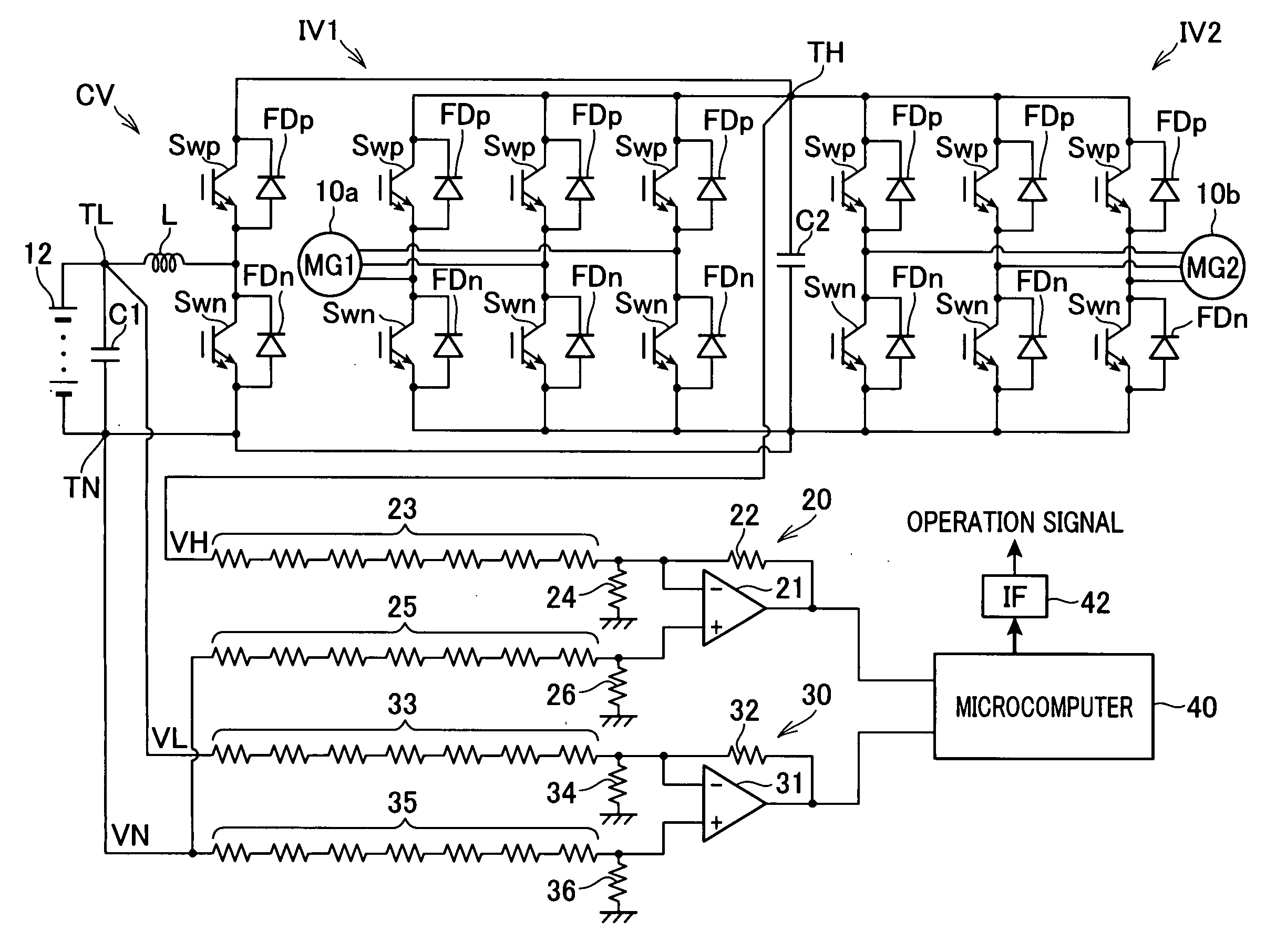
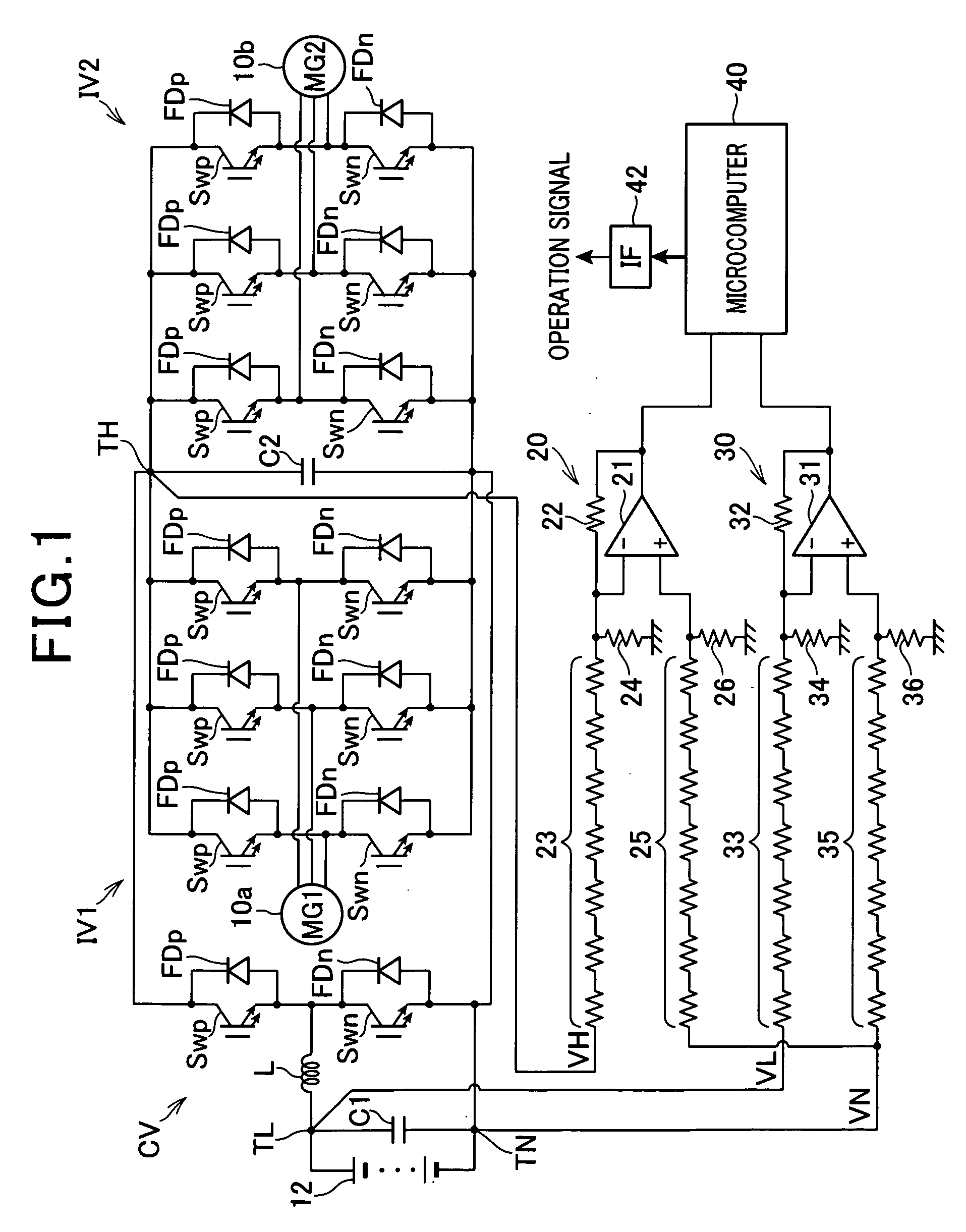
[0046]FIG. 1 shows a configuration of the power conversion circuit according to a first embodiment.
[0047]A first motor generator 10a and a second motor generator 10b shown in FIG. 1 are mechanically connected to a drive wheel and an internal combustion engine by a power divider. The first motor generator 10a is connected to an inverter IV1. The second motor generator 10b is connected to an inverter IV2. Here, the input voltages of the inverters IV1 and IV2 are the output voltage of a ...
second embodiment
[0067]A second embodiment will hereinafter be described with reference to FIG. 5, mainly focusing on differences from the first embodiment.
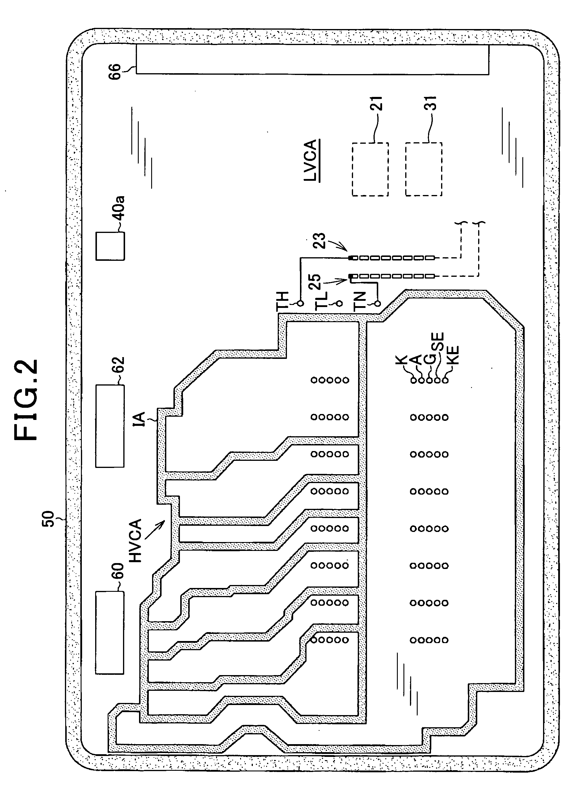
[0068]FIG. 5 shows the semiconductor substrate 50 according to the second embodiment. In FIG. 5, components corresponding to the components shown in FIG. 2 are given the same reference numbers for convenience.
[0069]As shown in FIG. 5, according to the second embodiment, the high-resistance resistors 23 are disposed along the insulating area IA. The high-resistance resistors 25 are disposed along the high-resistance resistors 23. Furthermore, according to the second embodiment, the terminals TH, TL, and TH are disposed along an edge section 50a of the semiconductor substrate 50 (i.e., belt-shape section covering a periphery of the semiconductor substrate 50). Here, the edge section of the semiconductor substrate 50 is an area in which components cannot ordinarily be disposed (shown in FIG. 5 as an area lighter in color than the insulating area IA)...
third embodiment
[0070]A third embodiment will hereinafter be described with reference to FIG. 6, mainly focusing on differences from the first embodiment.
[0071]FIG. 6 shows the semiconductor substrate 50 according to the third embodiment. In FIG. 6, components corresponding to the components shown in FIG. 2 are given the same reference numbers for convenience.
[0072]According to the third embodiment, the terminals TH, TL, and TN are disposed along the insulating area. The high-resistance resistors 23 are disposed along the edge section of the semiconductor substrate 50.
PUM
 Abstract
Description
Claims
Application Information
 - R&D
- Intellectual Property
- Life Sciences
- Materials
- Tech Scout
- Unparalleled Data Quality
- Higher Quality Content
- 60% Fewer Hallucinations
Browse by: Latest US Patents, China's latest patents, Technical Efficacy Thesaurus, Application Domain, Technology Topic, Popular Technical Reports.
© 2025 PatSnap. All rights reserved.Legal|Privacy policy|Modern Slavery Act Transparency Statement|Sitemap|About US| Contact US: help@patsnap.com


