
Methods of in-situ measurements of wafer bow

a wafer and insitu measurement technology, applied in the direction of electrical programme control, semiconductor/solid-state device testing/measurement, instruments, etc., can solve the problems of non-planar wafer, damage to the wafer and/or the upper electrode, and defective semiconductor devices being created

Active Publication Date: 2012-11-08
LAM RES CORP
View PDF12 Cites 10 Cited by
  • Summary
  • Abstract
  • Description
  • Claims
  • Application Information

AI Technical Summary

Benefits of technology

This solution provides accurate and efficient measurement of wafer bow and thickness, reducing the risk of defective products and processing errors, while minimizing the impact on overall processing time and resources, enabling more precise control over etching processes.

Problems solved by technology

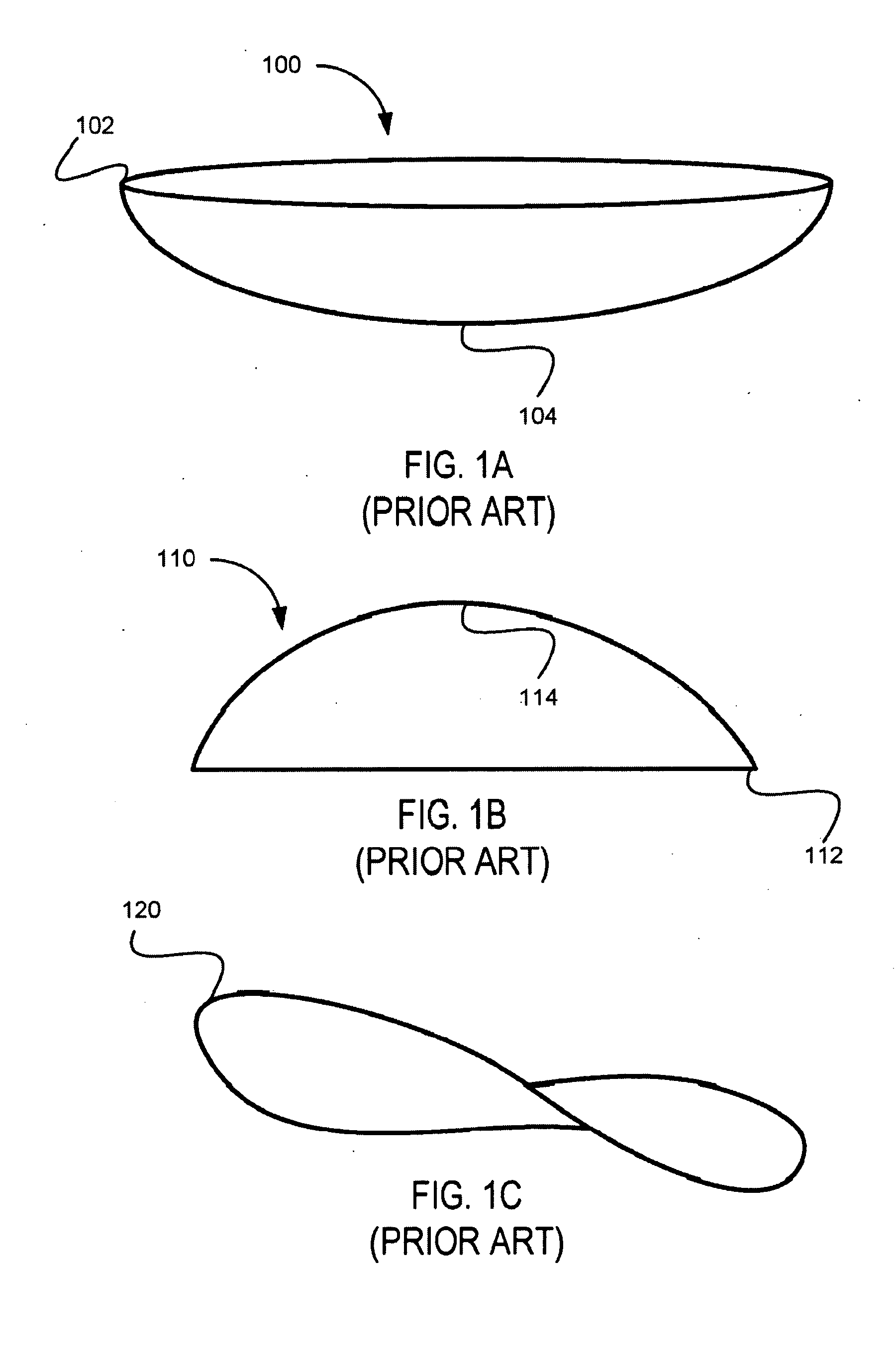
Since most recipes for processing the wafer assume that the wafer is planar, a non-planar wafer (e.g., a wafer with a bow) may cause variations that may result in defective semiconductor devices being created.
However, most wafers tend to have a slight bow and / or bump, thereby causing the wafer to be non-planar.
Thus, if the wafer bow is not correctly identified, the upper electrode may accidentally touch the wafer, thereby causing damages to the wafer and / or the upper electrode.
In addition, since the amount of plasma that may be introduced into the process module may also depend on knowing the actual gap, not being able to accurately identify the gap may cause variation in the processing.
However, in-line measurements are generally not taken during the deposition process.
Thus, measurement data may not be available to be fed into the etching process in order to determine the extent of the wafer bow.
In addition, since the stand-alone metrology tools are not in-situ or even in-line, the measurements data are usually not in a format that enables the data to be easily fed forward to another tool, such as a bevel etcher.
Unfortunately, the measurements that are taken are local to a single point, Thus, the measurements may not be the actual height of the wafer.
Since the processing steps require 0.1 millimeter (in this example) to perform the processing, but the upper electrode is actually 0.05 millimeters from the wafer, the wafer may inadvertently cause the wafer to be etched too deeply, which may cause a bad semiconductor devices to be created.
Thus, taking measurements at a single point may not be sufficient to determine the true minimal distance between the electrode and the wafer.
However, since the measurements are being performed as part of the processing steps, there is usually not sufficient time to take a sufficient sample to determine the true height of the wafer without negatively impacting the total processing time.
In addition, the prior art method does not provide for identifying the thickness of the wafer.
Since, the thickness can not be determined with a single point of measurement, the true gap between the upper electrode and the wafer may not be accurately determined.
As a result, variation may occur in processing that may result in a defective product.

Method used


Image

  • Methods of in-situ measurements of wafer bow
  • Methods of in-situ measurements of wafer bow
  • Methods of in-situ measurements of wafer bow

Examples


Embodiment Construction

[0030]The present invention will now be described in detail with reference to a few embodiments thereof as illustrated in the accompanying drawings. In the following description, numerous specific details are set forth in order to provide a thorough understanding of the present invention. It will be apparent, however, to one skilled in the art, that the present invention may be practiced without some or all of these specific details. In other instances, well known process steps and / or structures have not been described in detail in order to not unnecessarily obscure the present invention.

[0031]Various embodiments are described hereinbelow, including methods and techniques. It should be kept in mind that the invention might also cover articles of manufacture that includes a computer readable medium on which computer-readable instructions for carrying out embodiments of the inventive technique are stored. The computer readable medium may include, for example, semiconductor, magnetic, ...


PUM


Abstract

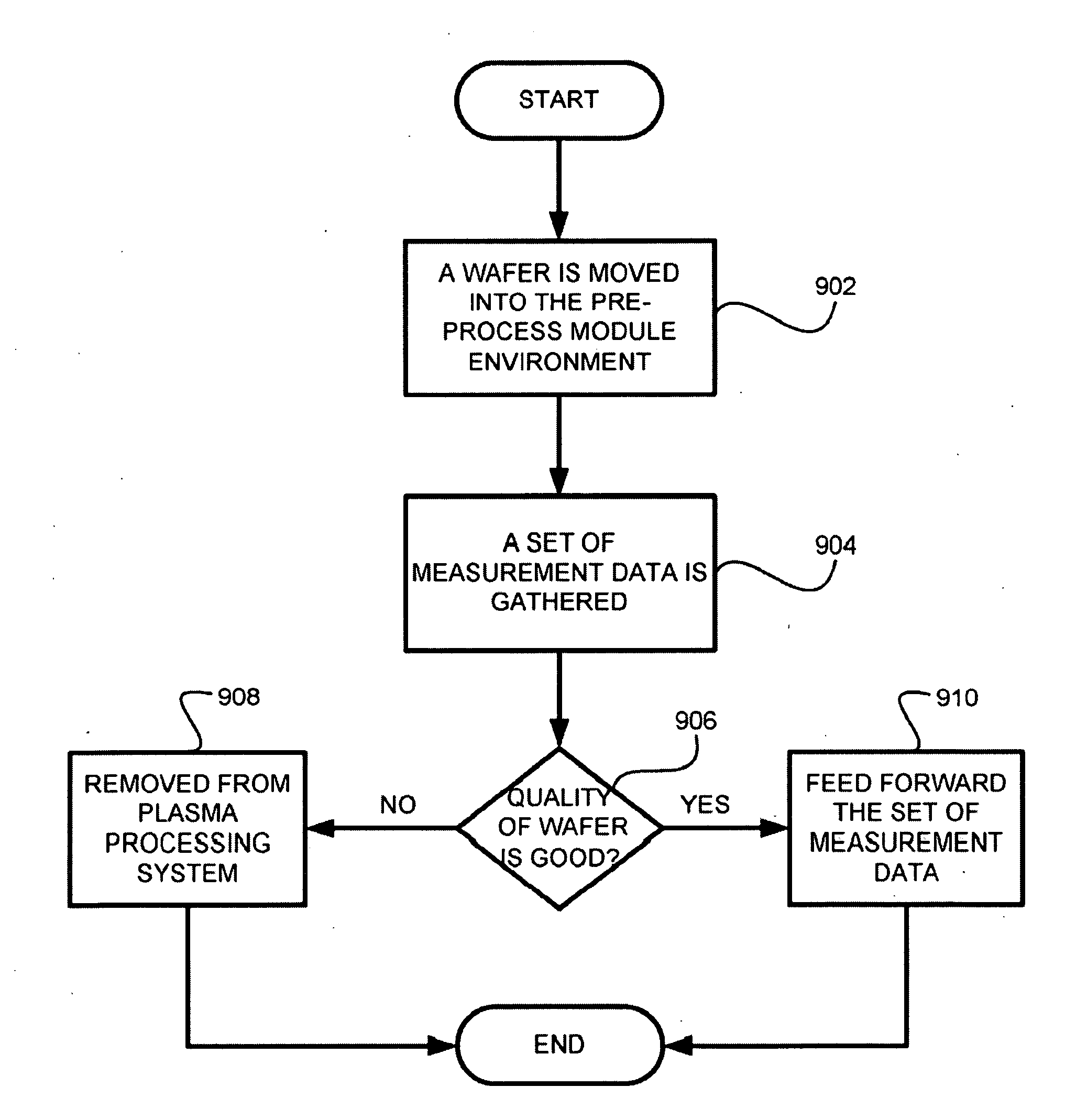
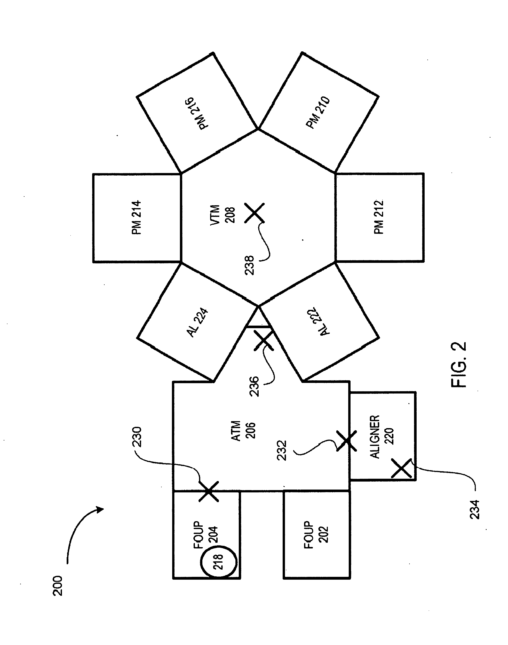
Various embodiments describe a method of quantifying bow in a wafer. In one embodiment, the method includes measuring a first plurality of distances from a first sensor to a first surface of the wafer to calculate the bow in the wafer. The first sensor is positioned outside of a set of process modules of the plasma processing system. A determination is made whether the calculated bow of the wafer is within a pre-determined range. If the calculated bow of the wafer is within the pre-determined range, the wafer is moved into a process module of the set of process modules for processing and a recipe for processing the wafer is adjusted based on the calculated bow of the wafer. If the calculated bow of the wafer is outside the pre-determined range, the wafer is removed from the plasma processing system. Other methods are described as well.

Description

[0001]This application is a divisional of and claims the benefit of priority under 35 U.S.C. §120 to U.S. patent application Ser. No. 12 / 233,501, filed on Sep. 18, 2008, which claims the benefit of priority under 35 U.S.C. §119(e) to U.S. Provisional Patent Application Ser. No. 60 / 976,149, filed on Sep. 28, 2007, the benefit of priority of each of which is claimed hereby, and each of which are incorporated by reference herein in its entirety.[0002]Advances in plasma processing have facilitated growth in the semiconductor industry. Usually, a plurality of semiconductor devices may be created from dies cut from a single processed wafer (i.e., substrate). Since most recipes for processing the wafer assume that the wafer is planar, a non-planar wafer (e.g., a wafer with a bow) may cause variations that may result in defective semiconductor devices being created.[0003]In an ideal situation, a wafer is perfectly planar. However, most wafers tend to have a slight bow and / or bump, thereby c...

Claims


Application Information

Patent Timeline
Patent Type & Authority Applications(United States)
IPC IPC(8): H01L21/66H01L21/677G05B19/19G06F19/00
CPCG01B21/30H01L21/68H01L22/12H01L22/20G01B21/08G01B21/20
Inventor BAILEY, III, ANDREW D.
Owner LAM RES CORP
Learn More