[0012]As a result, the RFID antenna is a
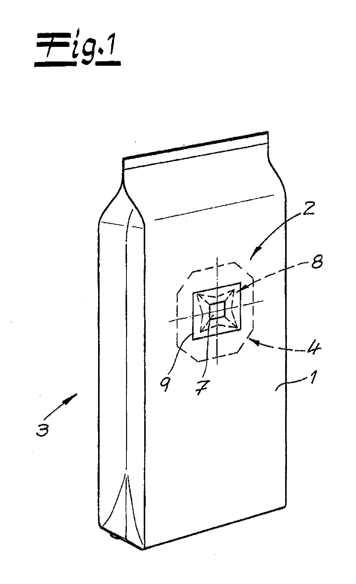
direct component of the packaging or of the molded part, and does not have to be applied with a correspondingly large
label. Only the support section with the RFID chip is applied separately, whereby the support section is usually clearly smaller than the antenna.
[0014]In the case of contact-free
coupling of the RFID antenna to the RFID chip, for example by way of the
adaptation network, the
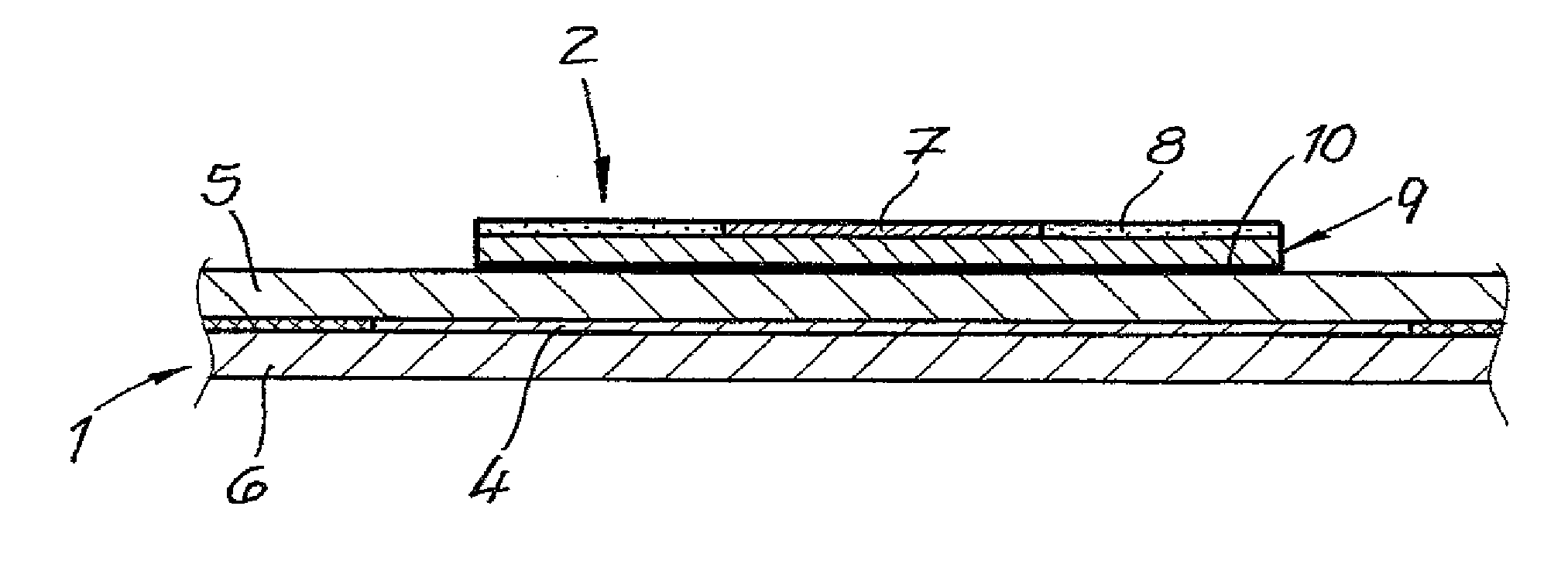
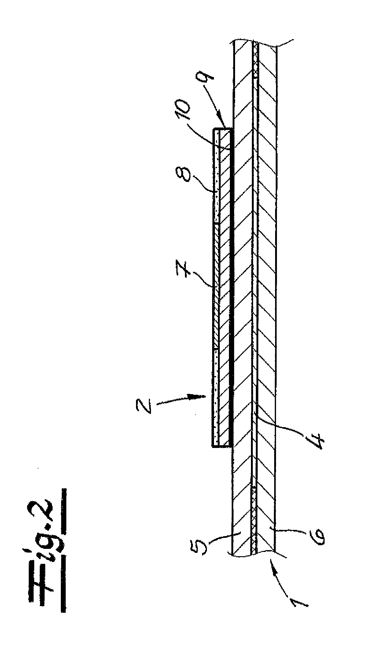
advantage is obtained that the antenna does not have to be disposed on the surface of the film. Thus, according to the invention, a multi-layer laminated film is made available, in which the antenna is disposed on a layer transition of the film that lies on the inside. The antenna is then optimally protected from mechanical damage. Thus, it is also easily possible to first print the antenna onto a film web before sections of the film are then processed to produce parts of a packaging or of a molded part. A gravure printing process is particularly suitable for printing the antenna onto the film web before such
processing. Reliable protection is also guaranteed during such
processing operations, which include
cutting, folding, and sealing, for example, when the RFID antenna is disposed on the inside. Even during subsequent handling of the body, the antenna cannot be damaged as the result of friction wear or other mechanical influences, if it is disposed to lie on the inside. In this connection, it should be taken into consideration that RFID antennas frequently have delicate conductor track structures, and thus are sensitive to damage to a certain degree. If, for example a conductor track is
cut, the usual emission characteristics are lost, whereby the characteristic frequency usually also changes completely.
[0015]Within the scope of the invention, the material composition of the film is not restricted further. The only thing that has to be guaranteed is that a layer of the film demonstrates sufficient imprintability. For the production of packagings, composite films composed of
polyethylene terephthalate and
polyethylene (PET / PE composite) are frequently used. In such composites, a decorative imprint is frequently provided at the layer transition that lies on the inside, on the layer of PET. The decorative imprint is then protected from friction wear, after lamination, with at least one further layer, particularly a layer of
polyethylene. The RFID antenna can also be applied on the inside, in the same printing process with a
conductive ink. Suitable printing inks are known, for example, from DE 10 2005 007 772 A1 and WO 03 / 068874 A1. Also with regard to the
aging resistance of the
printing ink, placement of the RFID antenna on a layer transition of the film that lies on the inside is particularly advantageous. Thus, for example, a
printing ink that contains silver can easily be used; such an ink is characterized by good electrical properties, but is sensitive to aging when placed in an exposed location. Accordingly, the configuration of the body according to the invention, with the antenna at a layer transition that lies on the inside, is also suitable for long-term storage or archiving of the objects to be identified. In other words, the configuration is suitable for long-term storage or archiving of the packaging or of the molded part.
[0017]The RFID chip is coupled with the RFID antenna by way of the
adaptation network, in the manner of an LC oscillation circuit. Proceeding from the connectors for the RFID chip, the adaptation network can therefore have conductor tracks and conductive surfaces. The conductor tracks essentially have the function of a coil, and the conductive surfaces essentially have the function of a
capacitor. The adaptation network is provided for adaptation of the complex impedances of RFID chip and RFID antenna, so that transmission losses are minimized. If a total
resonance is produced as the result of the adaptation by means of the adaptation network, a maximal
signal emission or sensitivity of the RFID arrangement is achieved. In the case of the preferred capacitative
coupling, it is practical if conductive surfaces assigned to one another are provided on the adaptation network and on the RFID antenna, which surfaces form a
capacitor with the material that is disposed in between.
[0018]Aside from the size of and the distance between the surfaces, the
electricity constant of the material disposed in between also has to be taken into consideration. When the RFID antenna is placed within a multi-layer film, the
layers present between the RFID antenna and the adaptation network therefore have to be taken into consideration in terms of their thickness and their dielectricity. Within the scope of the invention, capacitative
coupling is advantageous because in this way,
signal transmission with minimized transmission losses is possible, with a compact structure. Alternatively, however, it is fundamentally also possible to provide
inductive coupling between the adaptation network and the RFID antenna. In this case, conductor tracks or coil structures of adaptation network and RFID antenna that are assigned to one another must be provided.


