
High Density Magnetic Random Access Memory

a random access and magnetic technology, applied in the field of high density magnetic random access memory, can solve the problems of reducing the size of the mram cell, unable to provide the required spin-polarized current,

Active Publication Date: 2012-10-11
AGAN TOM A +1
View PDF5 Cites 27 Cited by
  • Summary
  • Abstract
  • Description
  • Claims
  • Application Information

AI Technical Summary

Benefits of technology

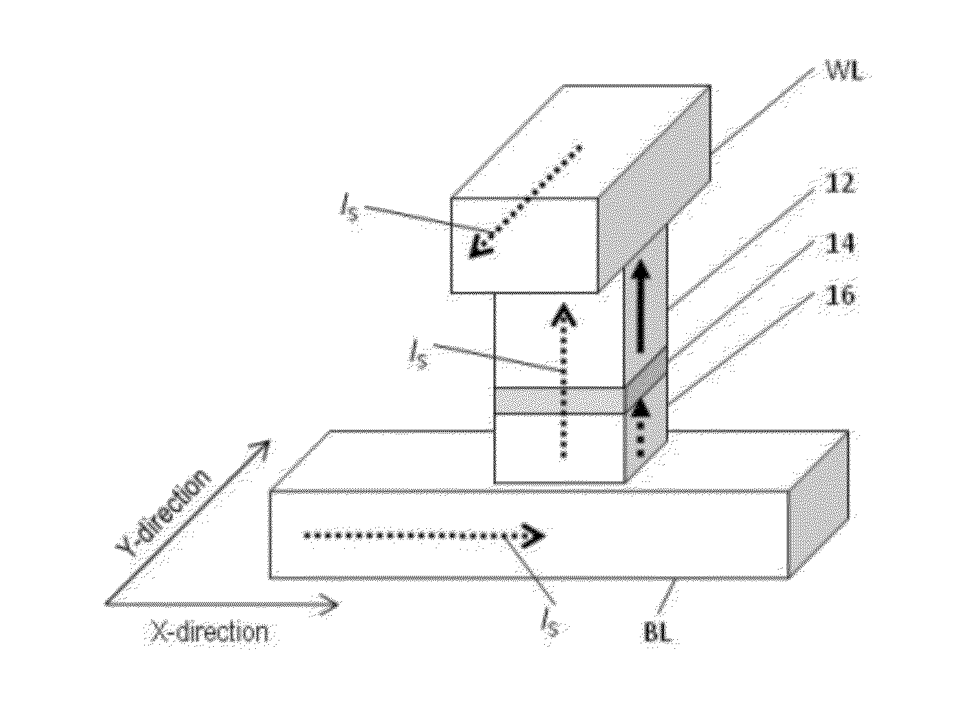
[0014]Also disclosed a method for writing to a magnetic memory device that includes a plurality of magnetic tunnel junctions formed on a substrate and arranged in columns and rows, each magnetic tunnel junction comprising a free ferromagnetic layer having a reversible magnetization direction directed substantially perpendicular to the substrate in an equilibrium state, a pinned ferromagnetic layer having a fixed magnetization direction, and an insulating tunnel barrier layer disposed between the free ferromagnetic layer and the pinned ferromagnetic layer, the method includes applying a bias current to a bit conductive line comprising ferromagnetic cladding and being electrically coupled to a row of magnetic tunnel junctions at the free ferromagnetic layer to produce a bias magnetic field along a hard magnetic axis of the free ferromagnetic layer, applying a first current to a conductive word line electrically coupled to a column of magnetic tunnel junctions at the pinned ferromagnetic layer to produce a spin momentum transfer in the free ferromagnetic layer of a magnetic tunnel junction located at a first intersection region of the bit conductive line and the word conductive line, wherein the bias current and the first current are applied at the same time, and a joint effect of the bias magnetic field and the spin momentum transfer causes a reversal of the magnetization direction of the free ferromagnetic layer of the magnetic tunnel junction located at the first intersection region.

Problems solved by technology

Frequently, especially for MR elements having in-plane magnetization in magnetic layers, one selection transistor cannot provide the required spin-polarized current due to its saturation.
This obstacle prevents the MRAM cell size reduction.

Method used


Image

  • High Density Magnetic Random Access Memory
  • High Density Magnetic Random Access Memory
  • High Density Magnetic Random Access Memory

Examples


Embodiment Construction

[0044]Embodiments of the present disclosure will be explained below with reference to the accompanying drawings. Note that in the following explanation the same reference numerals denote constituent elements having almost the same functions and arrangements, and a repetitive explanation will be made only when necessary.

[0045]Note also that each embodiment to be presented below merely discloses an device or method for embodying the technical idea of the present disclosure. Therefore, the technical idea of the present disclosure does not limit the materials, structures, arrangements, and the like of constituent parts to those described below. The technical idea of the present disclosure can be variously changed within the scope of the appended claims.

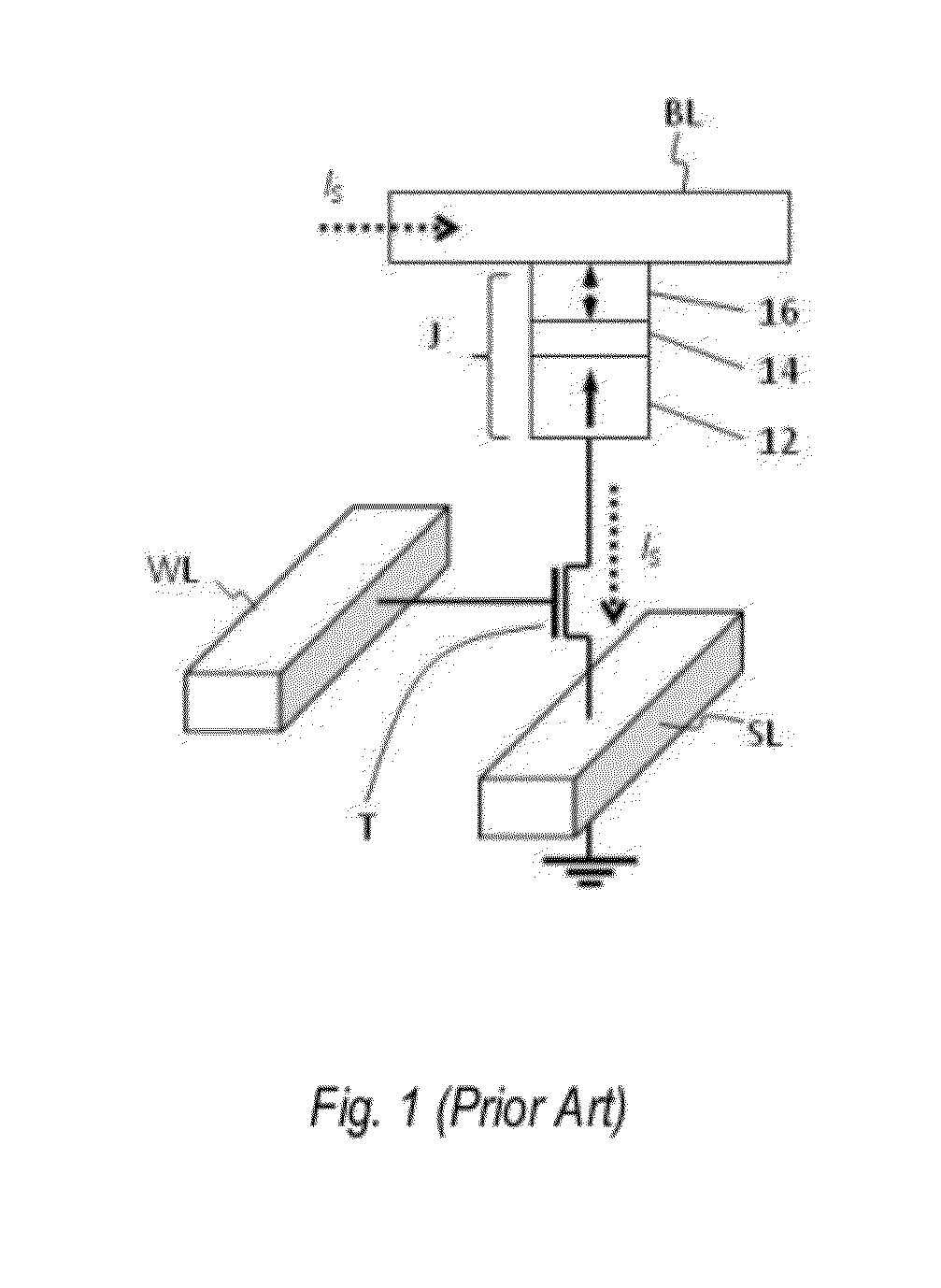
[0046]Refer now to the drawings, FIG. 1, FIG. 4, and FIG. 5 illustrate exemplary aspects of MR element. Specifically, these figures illustrate the MR element having a multilayer structure with a perpendicular direction of magnetization in...


PUM


Abstract

A magnetic memory device that comprises a substrate, a memory cell including a magnetic tunnel junction which comprises a free ferromagnetic layer having a reversible magnetization direction directed perpendicular to the substrate, a pinned ferromagnetic layer having a fixed magnetization direction directed perpendicular to the substrate, and an insulating tunnel barrier layer disposed between the pinned and free layers, a first electrical circuit for applying a first current to a first conductor electrically coupled to the free layer to produce a bias magnetic field along a hard axis of the free layer, a second electrical circuit for applying a second current to a second conductor electrically coupled to the pinned layer to cause a spin momentum transfer in the free layer, wherein magnitudes of the bias magnetic field and spin momentum transfer in combination exceed a threshold and thus reverse the magnetization direction of the free layer.

Description

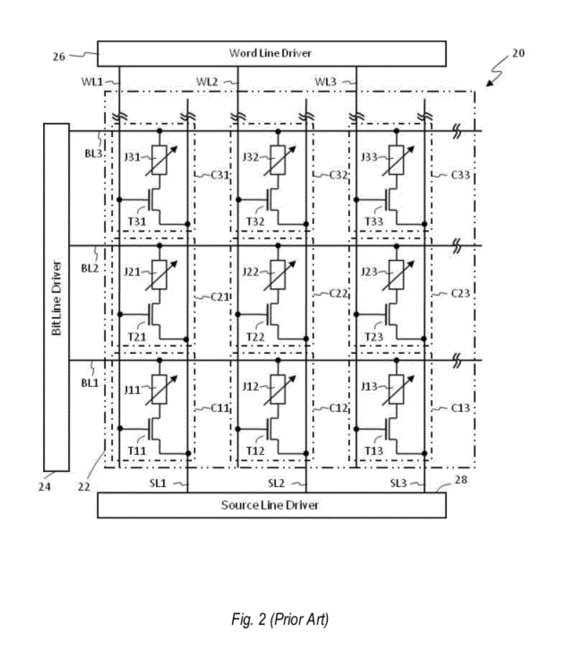
CROSS-REFERENCE TO RELATED APPLICATIONS[0001]This application claims the benefit of provisional patent application No. 61 / 472,788, filed on Apr. 7, 2011 by the present inventors.FEDERALLY SPONSORED RESEARCH[0002]Not ApplicableSEQUENCE LISTING OR PROGRAM[0003]Not ApplicableRELEVANT PRIOR ART[0004]U.S. Pat. No. 5,640,343, Jun. 17, 1997—Gallagher et al.[0005]U.S. Pat. No. 7, 224,601, May 29, 2007—Panchula[0006]U.S. Pat. No. 7,529,121, May 5, 2009—Kitagawa et al.BACKGROUND[0007]Magnetic random access memory (MRAM) using spin-induced switching is a strong candidate for providing a dense and fast non-volatile storage solution for future memory applications. Each MRAM includes an array of memory cells. FIG. 1 shows a schematic view of MRAM cell employing a spin-induced writing mechanism according to a prior art. The cell comprises a magnetoresistive element (or magnetic tunnel junction) J, a selection transistor T, a bit line BL, a word line WL, and a source line SL. The bit and word lines...

Claims


Application Information

Patent Timeline
Patent Type & Authority Applications(United States)
IPC IPC(8): G11C11/16
CPCG11C11/16G11C11/161G11C11/1673G11C11/1675
Inventor AGAN, TOM A.SHUKH, ALEXANDER MIKHAILOVICH
Owner AGAN TOM A
Learn More