
Optical sensor and method of manufacturing the optical sensor

a technology of optical sensors and manufacturing methods, applied in the field of optical sensors, can solve the problems of difficult downsizing and thinning, unstable posture of interposers and mounting boards, and deterioration of optical characteristics, so as to improve reliability, reduce manufacturing costs, and reduce manufacturing costs

Inactive Publication Date: 2012-10-04
ABLIC INC
View PDF2 Cites 1 Cited by
  • Summary
  • Abstract
  • Description
  • Claims
  • Application Information

AI Technical Summary

Benefits of technology

[0008]The present invention has been made in view of the above-mentioned circumstances, and has an object to provide a downsized and thinner optical sensor having excellent optical characteristics and improved reliability, and also provide a method of manufacturing the optical sensor with ease.

Problems solved by technology

Thus, there is a problem that it is difficult to achieve downsizing and thinning.
On the other hand, as exemplified in the photoelectric conversion device described in Japanese Patent Application Laid-open No. 2005-252041, if the interposer and the mounting substrate are supported by the solder bumps, the postures of the interposer and the mounting board become unstable depending on the shape of the solidified solder bumps.
If the interposer is tilted, the optical characteristics may be deteriorated.
Depending on the amount of the solder bump, the photoelectric conversion element may contact with the mounting board, and there is another problem that the reliability is lowered.
In addition, the photoelectric conversion element is not protected by a package or a resin, and hence the reliability may be deteriorated.
In this case, it is conceivable to seal a resin between the interposer and the mounting board, but the sealed resin lowers the light transmission characteristics, and further it is very difficult to seal a resin so as to avoid a photoelectric conversion portion of the photoelectric conversion element.
Besides, the resin may be colored with time to change the optical characteristics or moisture may permeate the resin to cause corrosion.
Thus, there is a problem that the reliability is insufficient.

Method used


Image

  • Optical sensor and method of manufacturing the optical sensor
  • Optical sensor and method of manufacturing the optical sensor
  • Optical sensor and method of manufacturing the optical sensor

Examples


Embodiment Construction

[0036]Hereinafter, an optical sensor and a method of manufacturing an optical sensor according to an embodiment of the present invention are described with reference to the accompanying drawings.

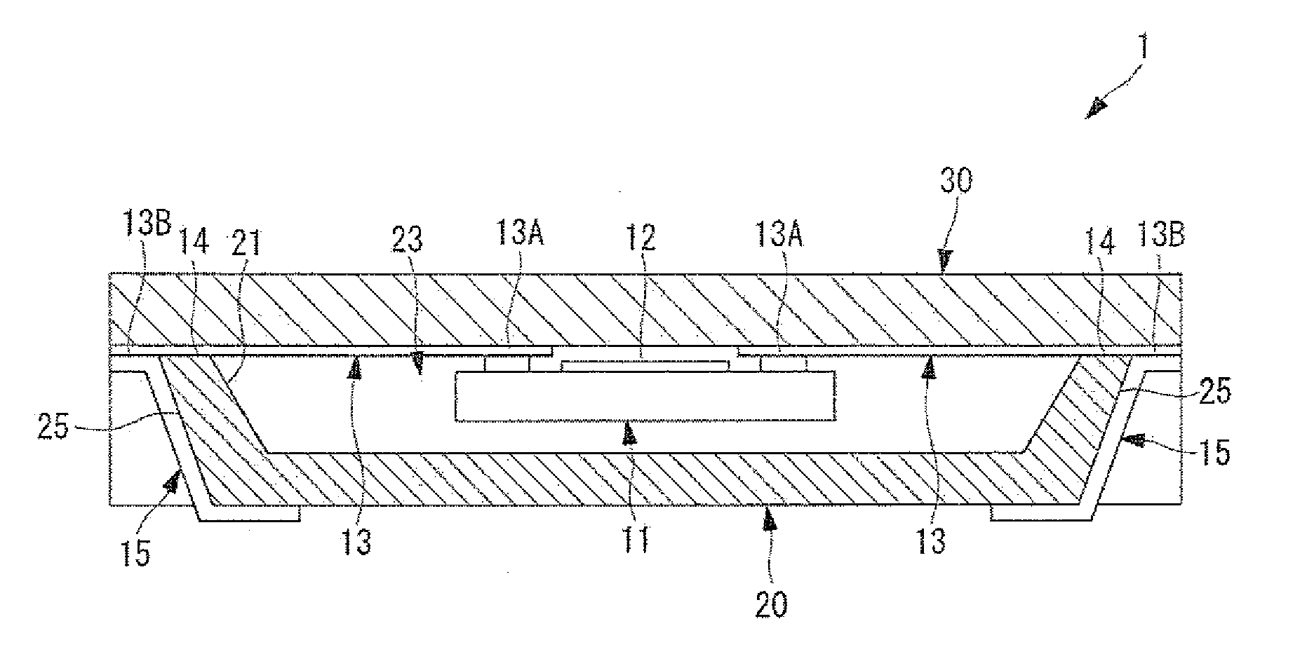
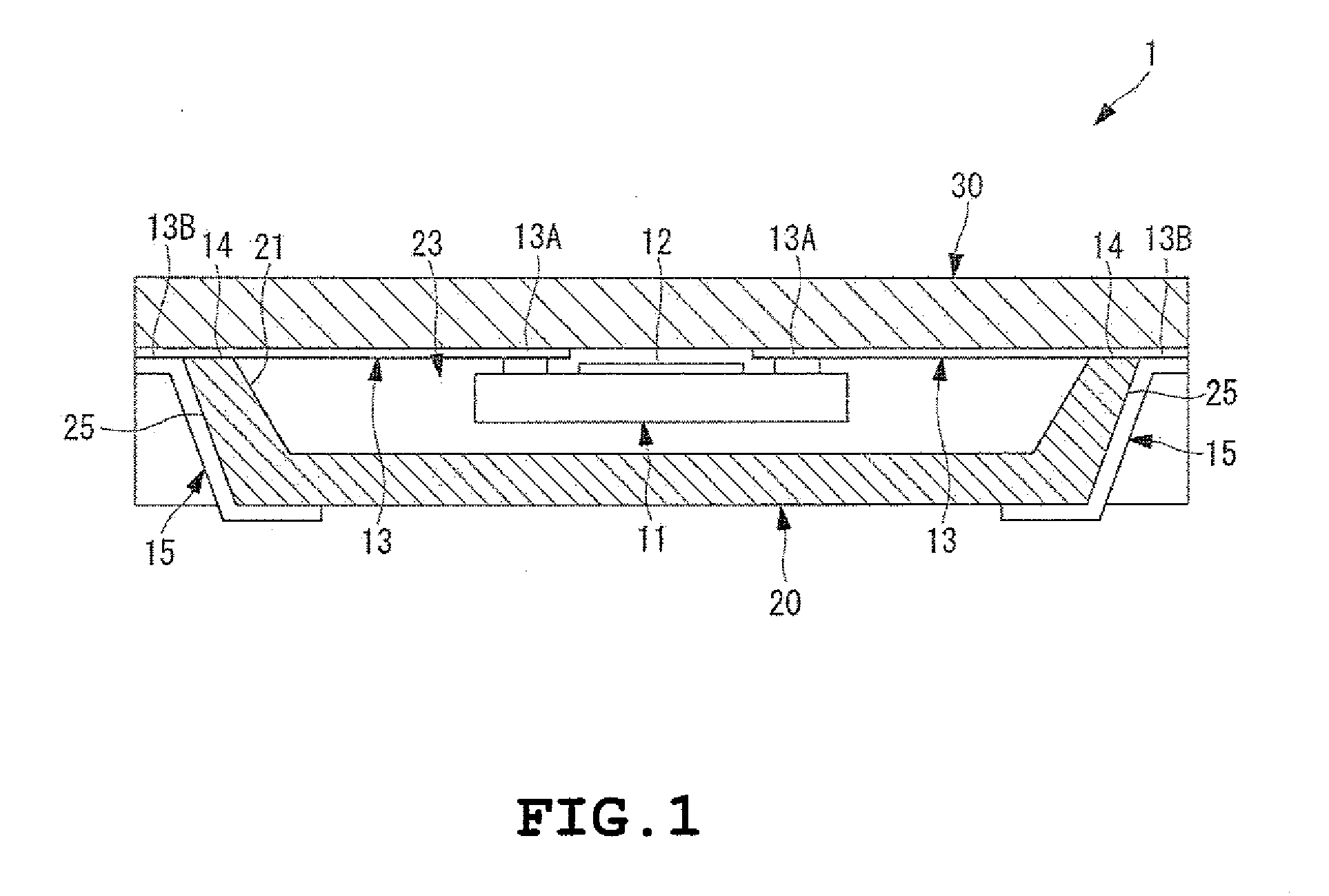
[0037]As illustrated in FIG. 1, an optical sensor 1 according to this embodiment includes a photoelectric conversion element (optical element) 11 for receiving light and detecting the intensity thereof, and the optical sensor 1 is thus capable of detecting ambient brightness. The optical sensor 1 is formed into, for example, a square with each side of 0.5 to 10 mm, and has a thickness of 0.2 to 1.5 mm. The optical sensor 1 has a structure in which a base 20 having a substantially plate shape and made of a glass material and a lid portion 30 having a flat plate shape and made of a transparent glass material on which the photoelectric conversion element 11 is mounted are bonded in a stacked state.

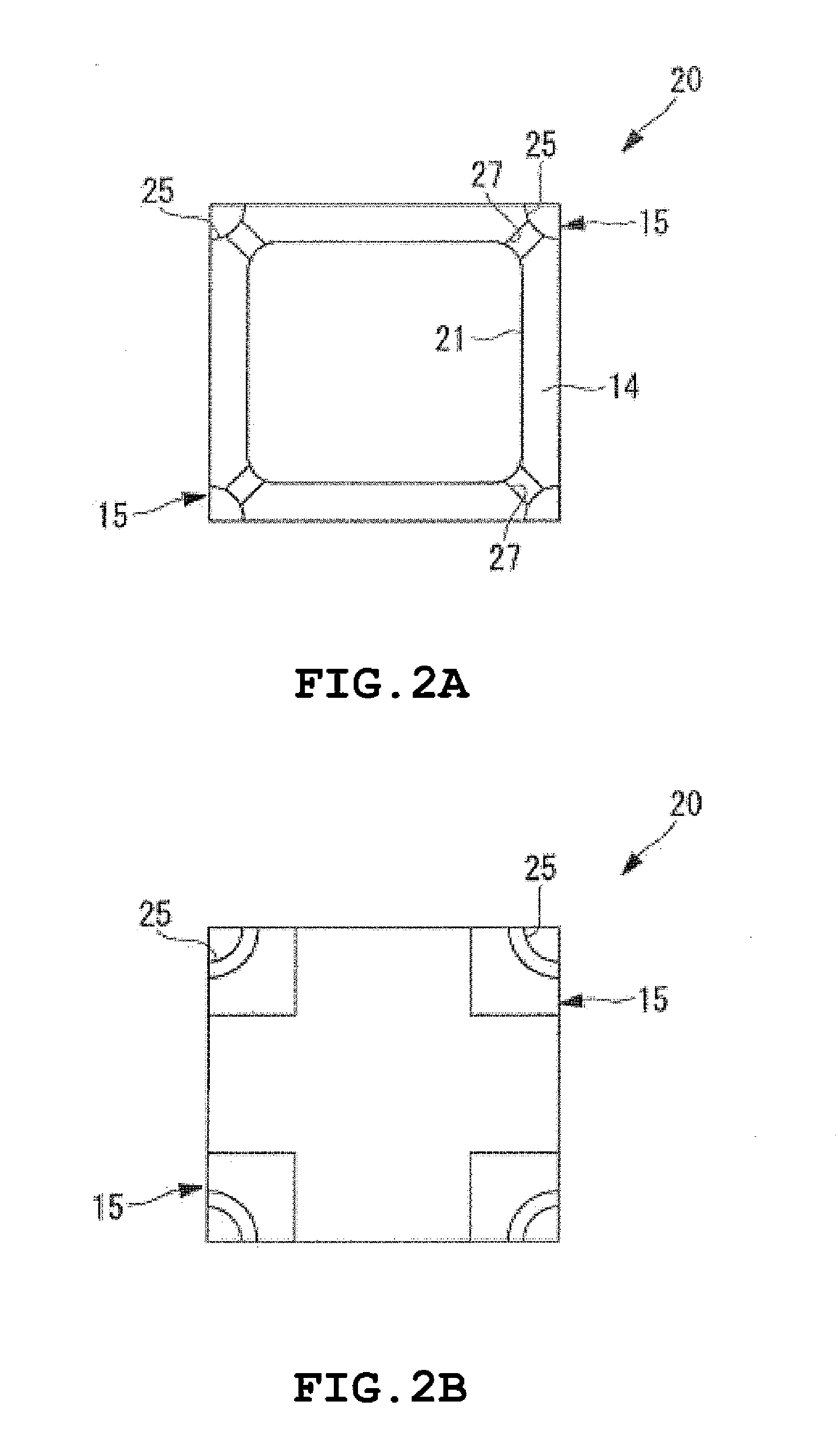
[0038]As illustrated in FIGS. 2A and 2B, the base 20 is formed into a square and has a thickness o...


PUM

PropertyMeasurementUnit
thicknessaaaaaaaaaa
thicknessaaaaaaaaaa
thicknessaaaaaaaaaa

Abstract

An optical sensor has a glass base having a concave portion, and a glass lid is bonded to the base and overlies the concave portion to form an hermetically sealed cavity portion. A photoelectric conversion element is accommodated in the cavity portion. Internal wirings are each connected at one end to the photoelectric conversion element and extend through notches formed in a peripheral edge of the base. The other ends of the internal wirings are connected inside the notches to external wirings that extend along an outside surface of the base and terminate in external terminals.

Description

BACKGROUND OF THE INVENTION[0001]1. Field of the Invention[0002]The present invention relates to an optical sensor and a method of manufacturing the same.[0003]2. Description of the Related Art[0004]Conventionally, there has been known an optical sensor including an optical element for detecting ambient brightness, which is used for dimming control in a television set or a mobile device monitor or for other purposes (see, for example, Japanese Patent Application Laid-open Nos. 2006-284474 and 2005-252041). In a photosensor (optical sensor) described in Japanese Patent Application Laid-open No. 2006-284474, a semiconductor chip (optical element) is accommodated in a package or is fixed onto a mounting board and covered by a transparent resin, and the semiconductor chip is connected to leads provided on the mounting board by bonding wires.[0005]In a photoelectric conversion device described in Japanese Patent Application Laid-open No. 2005-252041, using flip-chip bonding (FCB), a ligh...

Claims


Application Information

Patent Timeline
Patent Type & Authority Applications(United States)
IPC IPC(8): G01J1/04G01J3/51B23P17/04
CPCG01J1/0271G01J1/0214G01J1/0437H01L31/02002H01L31/0203G01J1/0488Y10T29/49826G01J1/0407G01J1/4204G01J5/045G01J5/041H01L2224/16225
Inventor TAKEUCHI, HITOSHIKIMURA, NORIYUKINOGUCHI, KOJI
Owner ABLIC INC
Learn More