
Parallelization of Error Analysis Circuitry for Reduced Power Consumption

a technology of error analysis and parallel configuration, applied in error detection/correction, instruments, coding, etc., can solve the problems of reliability, low cost and even lower margins, power consumption, etc., and achieve the effect of reducing power consumption, less parallel configuration, and greater power consumption

Active Publication Date: 2012-09-27
WESTERN DIGITAL ISRAEL LTD
View PDF3 Cites 10 Cited by
  • Summary
  • Abstract
  • Description
  • Claims
  • Application Information

AI Technical Summary

Benefits of technology

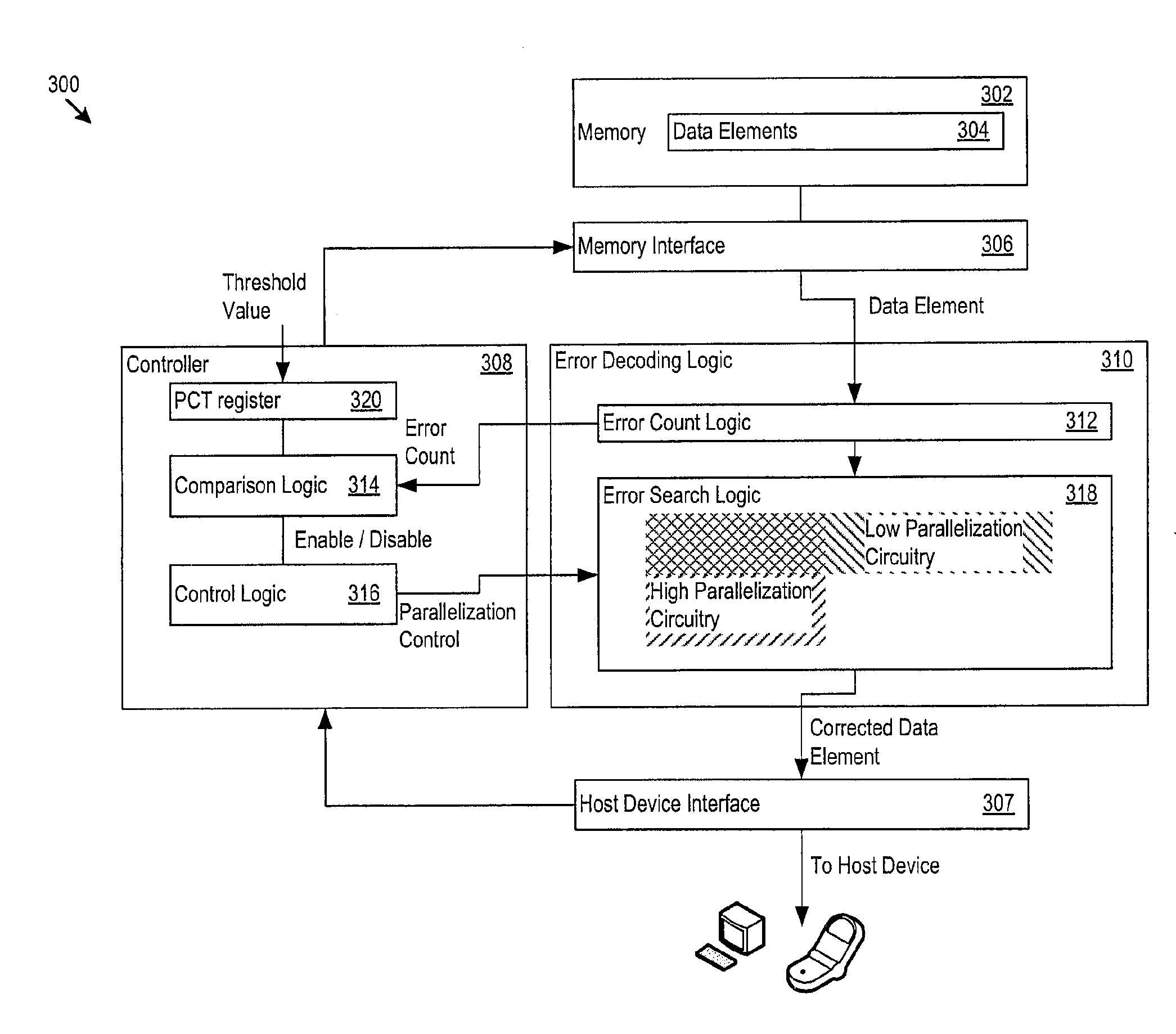
"The memory device described in this patent has a power-efficient error analysis circuitry that can detect and correct errors in code words before they are requested by a host device. The circuitry includes a highly parallel analysis section and a less parallel analysis section, with the less parallel section running less frequently to save power. The error analysis circuitry also includes an error search section that can test for errors in a code word and determine the error count. The error search section has a low parallelization circuit configuration and a high parallelization circuit configuration, depending on the error count. The controller in communication with the error search section can decide which circuit configuration to use for searching for errors. Overall, this design allows for efficient error analysis and correction in a memory device."

Problems solved by technology

One important characteristic of a memory device is its power consumption.
Significant volumes of memory devices are manufactured and sold each year, and competitive pressures have resulted in very low cost and even lower margins.
At the same time, low cost cannot be achieved at the expense of reliability.
However, when the error count does not exceed the parallelization threshold, the memory device searches for the errors with the high parallelization circuit configuration.

Method used


Image

  • Parallelization of Error Analysis Circuitry for Reduced Power Consumption
  • Parallelization of Error Analysis Circuitry for Reduced Power Consumption
  • Parallelization of Error Analysis Circuitry for Reduced Power Consumption

Examples


Embodiment Construction

[0018]The discussion below makes reference to host devices and memory devices. A host device may be a wired or wireless device, may be portable or relatively stationary, and may run from battery power, AC power, or another power source. A host device may be a consumer electronic device such as a personal computer, a mobile phone handset, a game device, a personal digital assistant (PDA), an email / text messaging device, a digital camera, a digital media / content player, a GPS navigation device, a satellite signal (e.g., television signal) receiver, or cable signal (e.g., television signal) receiver. In some cases, a host device accepts or interfaces to a memory device that includes the functionality described below. Examples of memory devices include memory cards, flash drives, and solid state disk drives. For example, a music / video player may accept a memory card that incorporates the functionality described below, or a personal computer may interface to a solid state disk drive that...


PUM


Abstract

A memory device (e.g., a flash memory device) includes power efficient codeword error analysis circuitry. The circuitry analyzes codewords stored in the memory of the memory device to locate and correct errors in the codewords before the codewords are communicated to a host device that requests the codewords from the memory device. The circuitry includes a highly parallel configuration with reduced complexity (e.g., reduced gate count) that a controller may cause to perform the error analysis under most circumstances. The circuitry also includes an analysis section of greater complexity with a less parallel configuration that the controller may cause to perform the error analysis less frequently. Because the more complex analysis section runs less frequently, the error analysis circuitry may provide significant power consumption savings in comparison to prior designs for error analysis circuitry.

Description

BACKGROUND OF THE INVENTION[0001]1. Technical Field[0002]This disclosure relates to error detection and correction of data stored in, for example memory devices employing, for example, flash memory. In particular, this disclosure relates to reducing the power consumption of error analysis circuitry in memory devices without substantially impacting error analysis performance.[0003]2. Related Art[0004]Continual development and rapid improvement in semiconductor manufacturing techniques have led to extremely high density memory devices. The memory devices are available in a wide range of types, speeds, and functionality. Memory devices often take the forms, as examples, of flash memory cards and flash memory drives. Today, capacities for memory devices have reached 64 gigabytes or more for portable memory devices such as Universal Serial Bus (USB) flash drives and one terabyte or more for solid state disk drives. Memory devices form a critical part of the data storage subsystem for dig...

Claims


Application Information

Patent Timeline
Patent Type & Authority Applications(United States)
IPC IPC(8): G11C29/08G06F11/07
CPCG06F11/1048H03M13/6561H03M13/3707H03M13/1545
Inventor DROR, ITAI
Owner WESTERN DIGITAL ISRAEL LTD
Learn More