Electro-optical device and electronic apparatus
a technology of optical devices and electronic devices, applied in the direction of instruments, static indicating devices, etc., can solve the problems of adversely affecting display quality, difficulty in producing holding capacitors with sufficient capacitance, and considerable decrease in holding voltag
- Summary
- Abstract
- Description
- Claims
- Application Information
AI Technical Summary
Benefits of technology
Problems solved by technology
Method used
Image
Examples
first embodiment
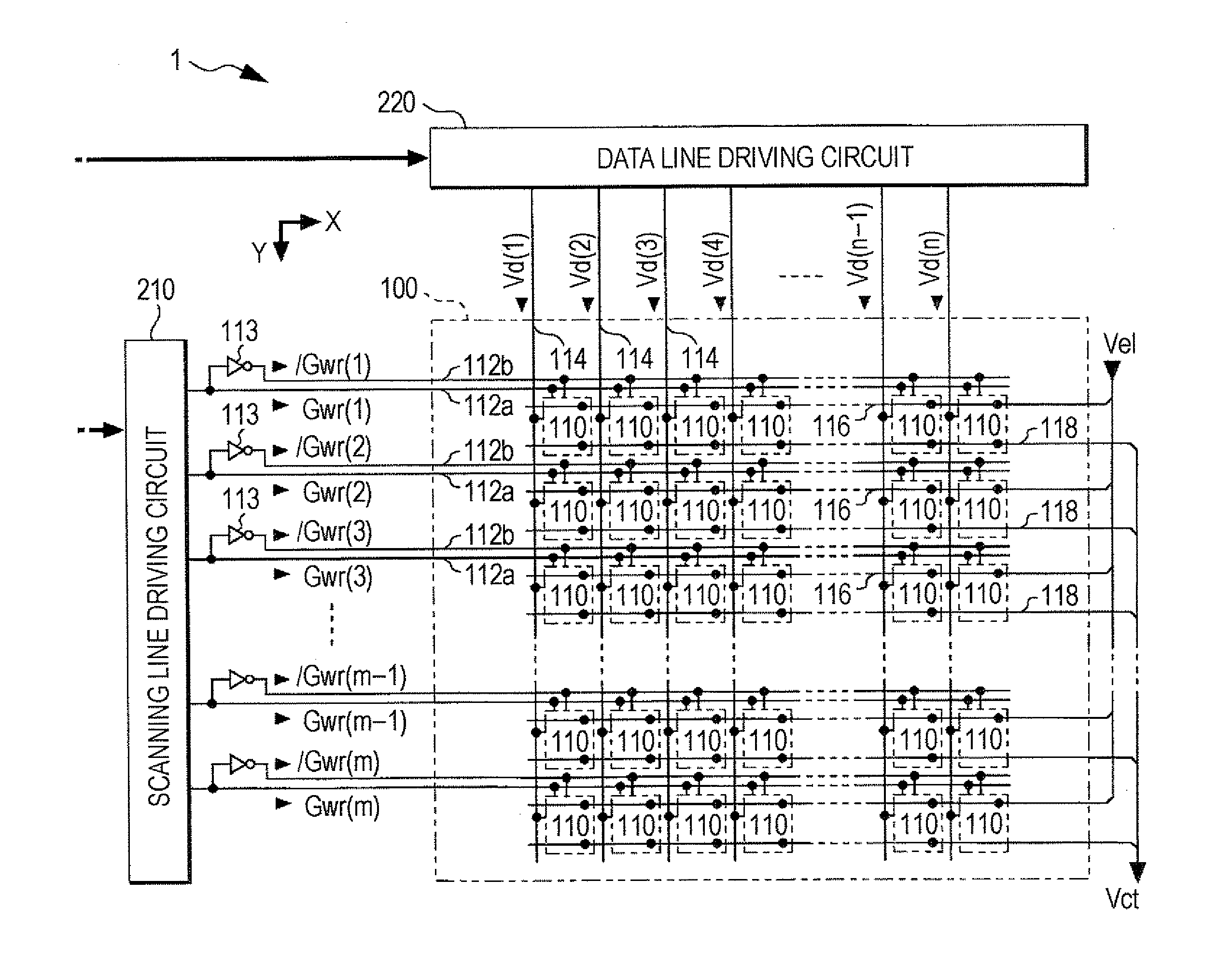
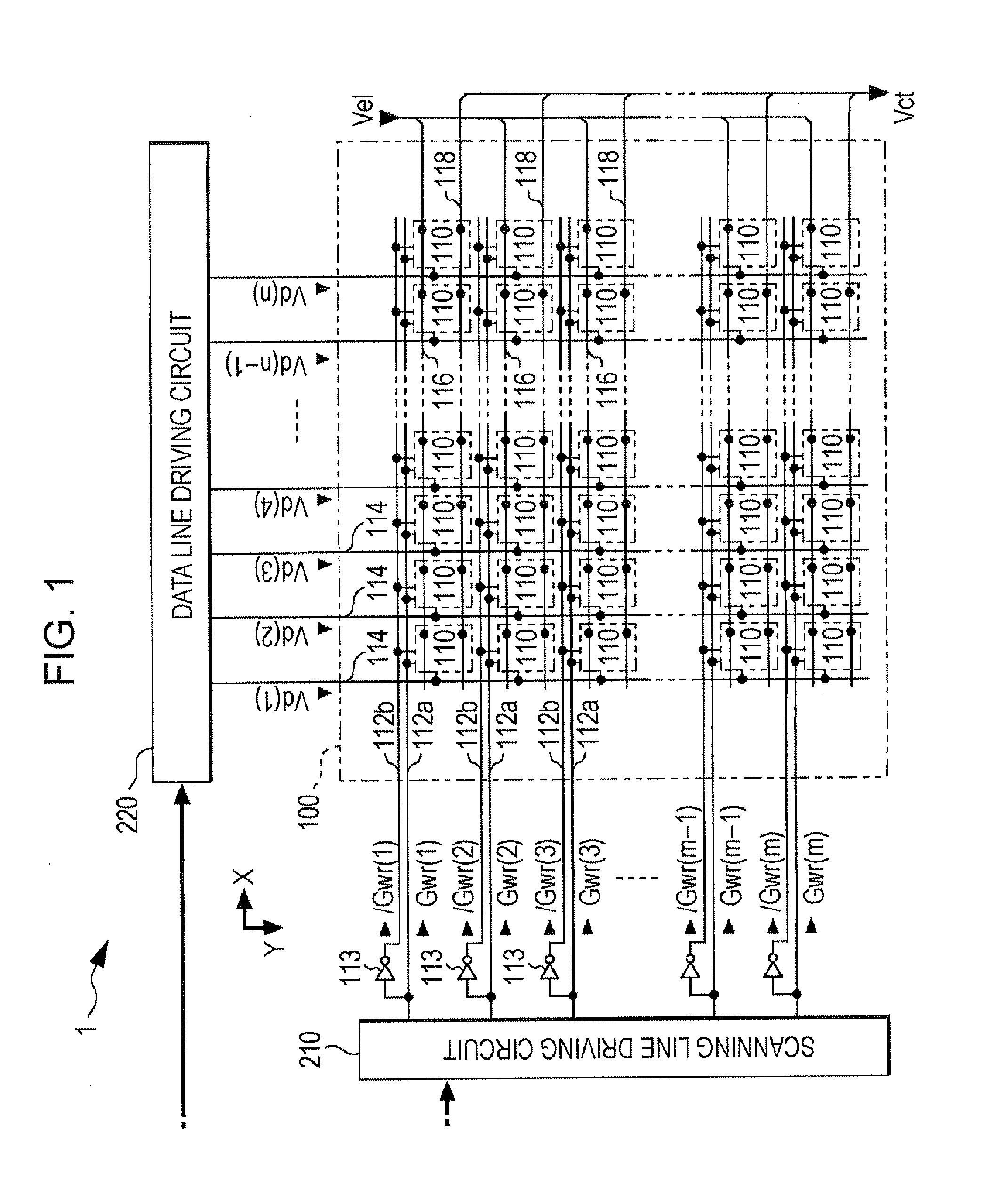
[0028]FIG. 1 is a block diagram showing the configuration of an electro-optical device 1 according to a first embodiment of the invention. An electro-optical device 1 is one which displays an image by using a plurality of pixel circuits 110.
[0029]As shown in FIG. 1, the electro-optical device 1 includes an element portion 100, a scanning line driving circuit 210, and a data line driving circuit 220.
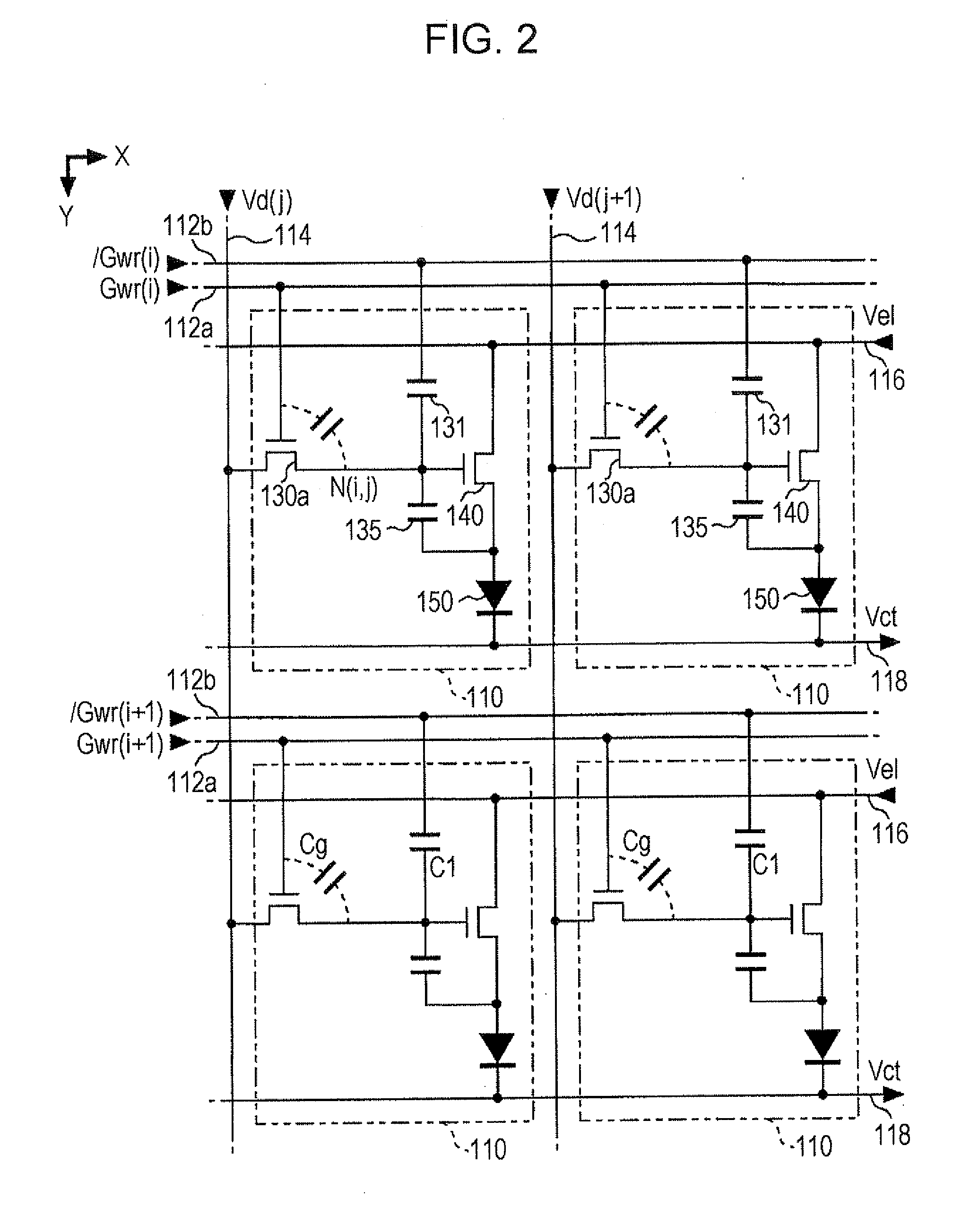
[0030]Among these, in the element portion 100, as shown in FIG. 1, scanning lines 112a of m rows are provided along the row (X) direction. Data lines 114 of n columns are provided along the column (Y) direction so as to maintain mutual electrical insulation with each scanning line 112a. The pixel circuits 110 are disposed so as to correspond to the intersections of scanning lines 112a of m rows and data lines 114 of n columns. Accordingly, in the present embodiment, the pixel circuits 110 are arranged in a matrix form with m rows vertically and n columns horizontally. In addition, both m ...
second embodiment
[0066]Next, a second embodiment of the invention will be described. FIG. 4 is a diagram showing an equivalent circuit in a pixel circuit of an electro-optical device according to the second embodiment.
[0067]In the pixel circuit shown in FIG. 4 compared to the first embodiment shown in FIG. 2, a capacitive element (second capacitive element) 132 is electrically interposed between the node N(i,j) and the scanning line 112a. In the second embodiment, when the capacitance of the capacitive element 132 is denoted as C2, the capacitance C1 of the capacitive element 131 is adjusted so as to be the sum of the capacitance C2 of the capacitive element 132 and the parasitic capacitance Cg of the transistor 130a.
[0068]Since the capacitance Cg is the parasitic capacitance of the transistor 130a, in practice, the capacitance Cg is minute. Thereby, unlike the first embodiment, it is considered that it is difficult to form the capacitive element 131 which is the same degree as the minute capacitan...
PUM
 Abstract
Description
Claims
Application Information
 - R&D
- Intellectual Property
- Life Sciences
- Materials
- Tech Scout
- Unparalleled Data Quality
- Higher Quality Content
- 60% Fewer Hallucinations
Browse by: Latest US Patents, China's latest patents, Technical Efficacy Thesaurus, Application Domain, Technology Topic, Popular Technical Reports.
© 2025 PatSnap. All rights reserved.Legal|Privacy policy|Modern Slavery Act Transparency Statement|Sitemap|About US| Contact US: help@patsnap.com


