
Atomic layer deposition of silicon nitride using dual-source precursor and interleaved plasma

Inactive Publication Date: 2012-08-23
APPLIED MATERIALS INC
View PDF6 Cites 173 Cited by
  • Summary
  • Abstract
  • Description
  • Claims
  • Application Information

AI Technical Summary

Benefits of technology

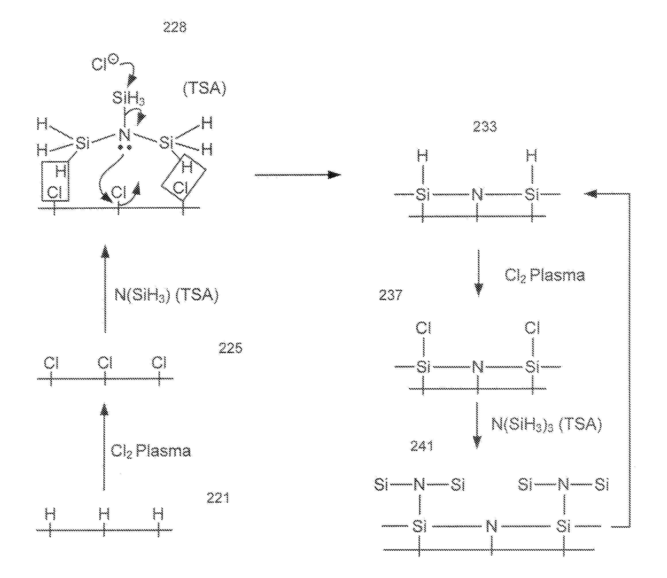
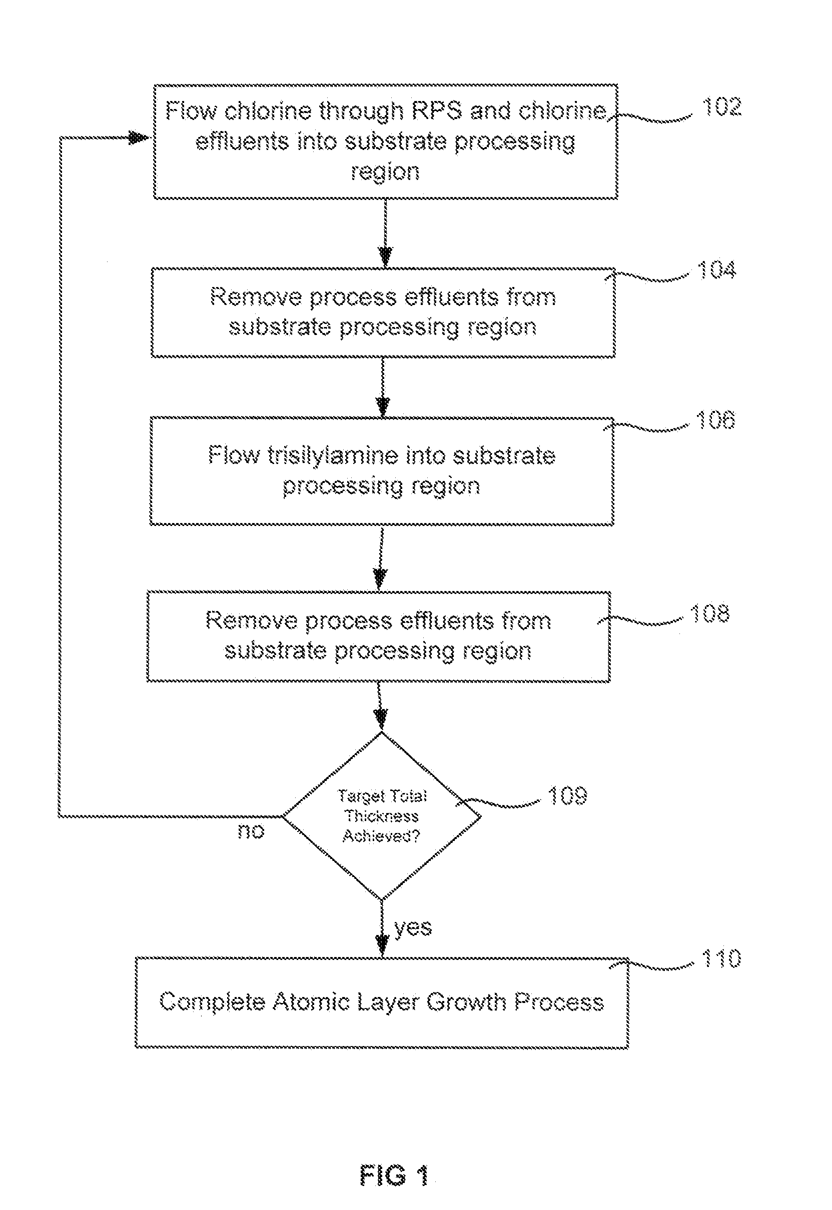
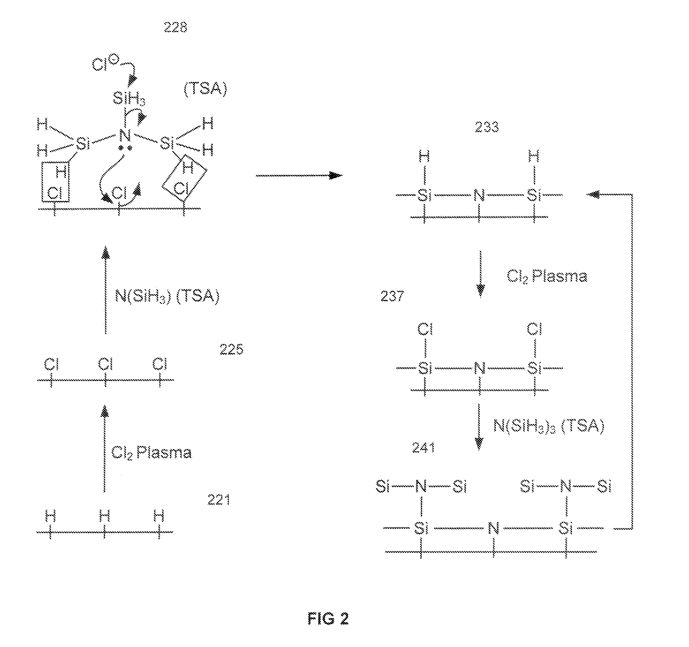
[0007]Atomic layer deposition using a precursor having both nitrogen and silicon components is described. The deposition precursor contains molecules which supply both nitrogen and silicon to a growing film of silicon nitride. Silicon-nitrogen bonds may be present in the precursor molecule, but hydrogen and / or halogens may also be present. The growth substrate may be terminated in a variety of ways and exposure to the deposition precursor displaces species from the outer layer of the growth substrate, replacing them with an atomic-scale silicon-and-nitrogen-containing layer. The silicon-and-nitrogen-containing layer grows until one complete layer is produced and then stops (self-limiting growth kinetics). Subsequent exposure to a plasma excited gas modifies the chemical termination of the surface so the growth step may be repeated. The presence of both silicon and nitrogen in the deposition precursor molecule increases the deposition per cycle thereby reducing the number of precursor exposures to grow a film of the same thickness.

Problems solved by technology

There are two conventional methods for depositing a silicon nitride film: (1) plasma-enhanced chemical vapor deposition (PECVD) at substrate temperatures of more than 250° C.; and (2) low-pressure chemical vapor deposition (LPCVD) process at a substrate temperature generally greater than 750° C. While satisfactory for larger integrated circuit linewidths, these methods can cause diffusion at interfaces due to the high deposition temperature.
Diffusion may degrade the integrity or inertness of silicon nitride films and may even degrade electrical characteristics of miniature electrical devices.
The silicon monolayer is terminated with chlorine and further exposure to Si2Cl4 results in insignificant additional deposition.
This second deposition step is also self-limiting; further exposure to H2O results in little additional deposition.
Prior art deposition methods, such as this, are limited to substrate temperatures above 100° C. and relatively low precursor reaction rates.

Method used


Image

  • Atomic layer deposition of silicon nitride using dual-source precursor and interleaved plasma
  • Atomic layer deposition of silicon nitride using dual-source precursor and interleaved plasma
  • Atomic layer deposition of silicon nitride using dual-source precursor and interleaved plasma

Examples


Embodiment Construction

[0015]Atomic layer deposition using a precursor having both nitrogen and silicon components is described. The deposition precursor contains molecules which supply both nitrogen and silicon to a growing film of silicon nitride. Silicon-nitrogen bonds may be present in the precursor molecule, but hydrogen and / or halogens may also be present. The growth substrate may be terminated in a variety of ways and exposure to the deposition precursor displaces species from the outer layer of the growth substrate, replacing them with an atomic-scale silicon-and-nitrogen-containing layer. The silicon-and-nitrogen-containing layer grows until one complete layer is produced and then stops (self-limiting growth kinetics). Subsequent exposure to a plasma excited gas modifies the chemical termination of the surface so the growth step may be repeated. The presence of both silicon and nitrogen in the deposition precursor molecule increases the deposition per cycle thereby reducing the number of precurso...


PUM

PropertyMeasurementUnit
Timeaaaaaaaaaa
Pressureaaaaaaaaaa
Widthaaaaaaaaaa

Abstract

Atomic layer deposition using a precursor having both nitrogen and silicon components is described. The deposition precursor contains molecules which supply both nitrogen and silicon to a growing film of silicon nitride. Silicon-nitrogen bonds may be present in the precursor molecule, but hydrogen and / or halogens may also be present. The growth substrate may be terminated in a variety of ways and exposure to the deposition precursor displaces species from the outer layer of the growth substrate, replacing them with an atomic-scale silicon-and-nitrogen-containing layer. The silicon-and-nitrogen-containing layer grows until one complete layer is produced and then stops (self-limiting growth kinetics). Subsequent exposure to a plasma excited gas modifies the chemical termination of the surface so the growth step may be repeated. The presence of both silicon and nitrogen in the deposition precursor molecule increases the deposition per cycle thereby reducing the number of precursor exposures to grow a film of the same thickness.

Description

CROSS-REFERENCES TO RELATED APPLICATIONS[0001]This application claims the benefit of U.S. Prov. Pat. App. No. 61 / 389,344 filed Oct. 4, 2010, and titled “ATOMIC LAYER DEPOSITION OF SILICON NITRIDE USING DUAL-SOURCE PRECURSOR AND INTERLEAVED PLASMA,” which is incorporated herein by reference in its entirety for all purposes.BACKGROUND OF THE INVENTION[0002]Silicon nitride dielectric films are used as etch stops and chemically inert diffusion barriers. Other applications benefit from the relatively high dielectric constant, which allows electrical signals to be rapidly transmitted through a silicon nitride layer. There are two conventional methods for depositing a silicon nitride film: (1) plasma-enhanced chemical vapor deposition (PECVD) at substrate temperatures of more than 250° C.; and (2) low-pressure chemical vapor deposition (LPCVD) process at a substrate temperature generally greater than 750° C. While satisfactory for larger integrated circuit linewidths, these methods can cau...

Claims


Application Information

Patent Timeline
IPC IPC(8): B05D3/04
CPCC23C16/345C23C16/45534H01L21/0228H01L21/0217H01L21/02274C23C16/45542
Inventor MALLICK, ABHIJIT BASU
Owner APPLIED MATERIALS INC
Learn More