
Variable capacitance device

a variable capacitance and capacitor technology, applied in the direction of variable capacitors, mechanically variable capacitors, capacitors, etc., can solve the problems of unstable variable capacitance and complex circuit structure of variable capacitance devices

Active Publication Date: 2012-08-16
MURATA MFG CO LTD
View PDF4 Cites 1 Cited by
  • Summary
  • Abstract
  • Description
  • Claims
  • Application Information

AI Technical Summary

Benefits of technology

[0008]To overcome the problems described above, preferred embodiments of the present invention provide a variable capacitance device that properly operates at a point along a signal line through which a high-voltage RF signal passes while the necessary DC voltage is controlled to remain constant or substantially constant.
[0010]With this configuration, the beam is deformed in accordance with a DC voltage in the drive capacitance generating portion, and a capacitance in the signal capacitance generating portion is changed accordingly. When the first substrate side signal electrode portion and the second substrate side signal electrode portion are connected to a signal line through which a high-voltage RF signal passes, an electrostatic force acts between the beam side signal electrode portion and the first and second substrate side signal electrode portions. The signal capacitance generating potion preferably has a structure (hereinafter called an MIMIM structure) in which an RF signal propagates between the first and second substrate side signal electrode portions, which are coupled to each other through the beam side signal electrode portion, and an electrostatic force is effectively reduced due to the structure. Thus, by providing the signal capacitance generating portion separately from the drive capacitance generating portion, only an electrostatic force that acts on the signal capacitance generating portion can be reduced or minimized, while ensuring that an adequate electrostatic force acts on the drive capacitance generating portion. As a result, the variable capacitance device properly operates at a point along a signal line through which a high-voltage RF signal passes.
[0016]With a cantilever structure, the spring constant of the beam and an area occupied by the beam are reduced as compared to a doubly supported beam. When the spring constant is reduced, the beam can be easily deformed and a relatively large capacitance can be generated using a relatively low DC voltage in the drive capacitance generating portion. In other words, a necessary electrostatic force can be generated using a relatively low DC voltage.
[0020]When the cross-sectional area of the beam is discontinuous rather than constant, a necessary capacitance can be obtained by locally increasing an opposing electrodes area in the beam. However, the beam is likely to become inclined as the beam gets closer to the substrate, whereby a change in capacitance may be unstable. Thus, by providing a configuration in which a plurality of portions having a relatively small cross-sectional area are arranged along the axis direction, the inclination when the beam gets closer to the substrate is reduced, whereby the stability of the change in capacitance is improved.
[0023]According to various preferred embodiments of the present invention, since the signal capacitance generating portion having an MIMIM structure is provided separately from the drive capacitance generating portion, only an electrostatic force produced by the signal capacitance generating portion which causes deformation of the beam can be reduced or minimized while ensuring that a sufficient electrostatic force still acts on the drive capacitance generating portion. As a result, the variable capacitance device operates properly at a point along a signal line through which a high-voltage RF signal passes.

Problems solved by technology

This electrostatic force prevents proper deformation of the beam structure due to a DC voltage and, thus, the variable capacitance becomes unstable.
As a result, for example, a voltage step-up circuit is required and the circuit structure of the variable capacitance device becomes more complex.

Method used


Image

  • Variable capacitance device
  • Variable capacitance device
  • Variable capacitance device

Examples


Embodiment Construction

[0035]An exemplary configuration of a variable capacitance device according to a first preferred embodiment of the present invention will be described below.

[0036]FIG. 2A is a plan view of a variable capacitance device 1. FIG. 2B is a cross-sectional side view of the variable capacitance device 1. FIG. 2C is an equivalent circuit diagram of the variable capacitance device 1.

[0037]The variable capacitance device 1 preferably includes a substrate 2, lower drive electrodes 3A, 3B, 4A, and 4B, a beam 6, and a dielectric layer 5. The substrate 2 is preferably a glass substrate and the beam 6 is preferably made of a low-resistance Si substrate (conductive material) with a resistivity of 0.0026 Ω-cm, for example. The dopant used is preferably P (phosphorus), but may be As (arsenic) or B (boron), for example.

[0038]The beam 6 is preferably shaped like a flat plate with an opening, and includes two beam-shaped portions 6B, a movable portion 6A, and a support portion 6C. The support portion 6C...


PUM


Abstract

A variable capacitance device that operates properly at a point along a signal line through which a high-voltage RF signal passes while reducing a necessary DC voltage includes a substrate, a beam, and lower drive electrodes. The beam is connected to the substrate through a support portion. Lower drive electrodes and the beam generate a capacitance when a DC voltage is applied, and an electrostatic force due to this capacitance deforms the beam. The lower drive electrodes face the beam and are coupled to each other through the beam. An RF signal propagates between the lower drive electrodes.

Description

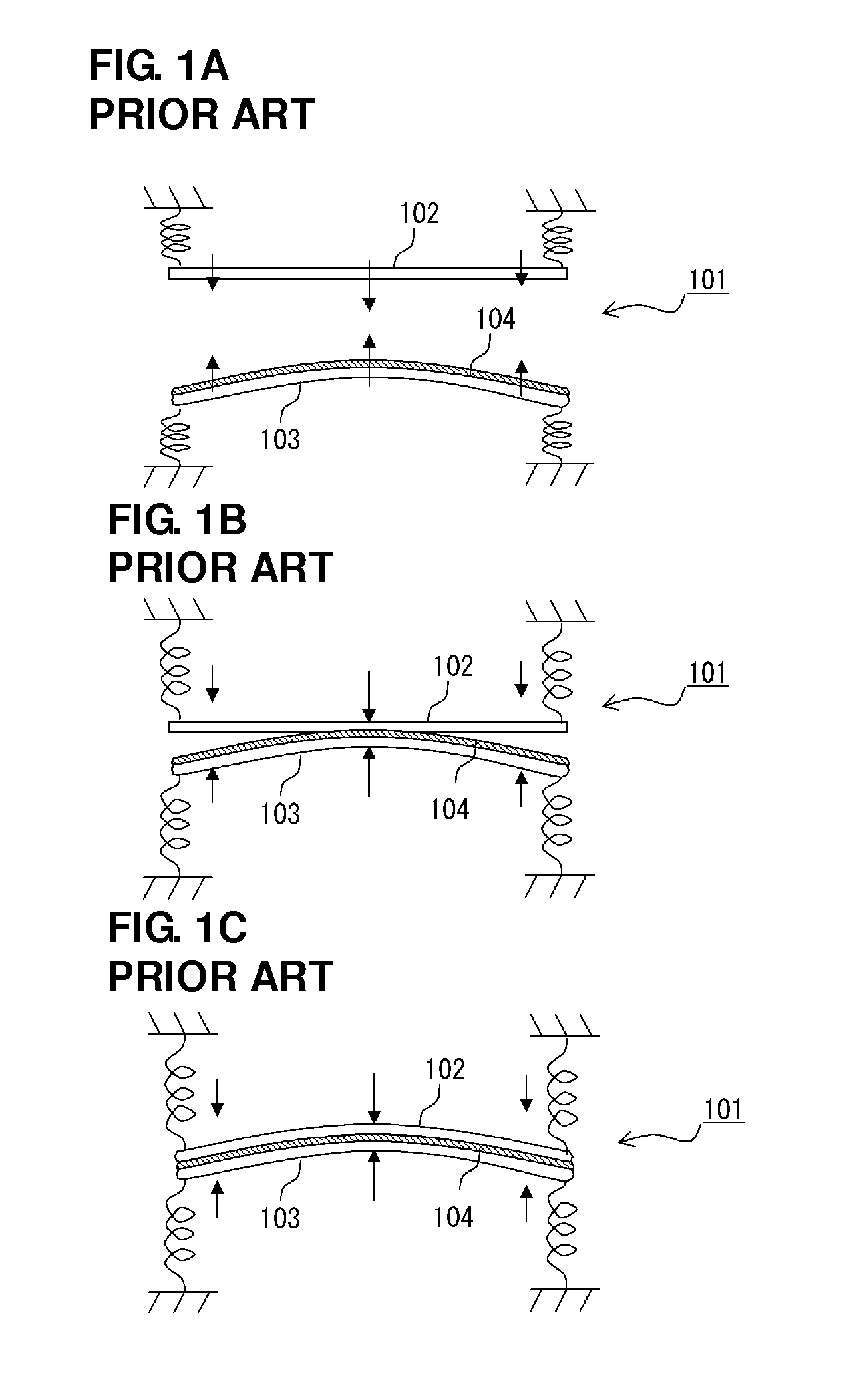
BACKGROUND OF THE INVENTION[0001]1. Field of the Invention[0002]The present invention relates to variable capacitance devices that change a capacitance using a microelectromechanical system (MEMS) component driven by an electrostatic force.[0003]2. Description of the Related Art[0004]Recently, some variable capacitance devices use a MEMS component that is driven by an electrostatic force (refer to Japanese Unexamined Patent Application Publication No. 2006-210843 and Japanese Unexamined Patent Application Publication No. 2008-182134).[0005]FIGS. 1A to 1C illustrate an exemplary configuration of an existing variable capacitance device.[0006]A variable capacitance device 101 includes movable plates 102 and 103. The movable plates 102 and 103, which have a double supported beam structure made of a conductive material, are arranged so as to be opposite each other. The movable plate 103 has a convex surface that is provided with a dielectric layer 104 and faces the movable plate 102. Whe...

Claims


Application Information

Patent Timeline
Patent Type & Authority Applications(United States)
IPC IPC(8): H01G7/06
CPCH01G5/18H01G5/011
Inventor UMEDA, KEIICHISHIBAHARA, TERUHISAYAMADA, HIROSHI
Owner MURATA MFG CO LTD
Learn More