Printed circuit board and method of manufacturing the same

a printed circuit board and manufacturing method technology, applied in the field of printed circuit boards, can solve the problems of adhesion between the insulating material and the conductive layer, and achieve the effect of ensuring adhesion

Inactive Publication Date: 2012-05-24
SAMSUNG ELECTRO MECHANICS CO LTD
View PDF4 Cites 10 Cited by
  • Summary
  • Abstract
  • Description
  • Claims
  • Application Information

AI Technical Summary

Benefits of technology

[0011]An aspect of the present invention provides a printed circuit board allowing for the formation of a fine pattern by securing a uniform roughness on an insulating layer and securing adhesion between a conductive layer and the insulating layer.

Problems solved by technology

However, in this case, a problem may arise in which the adhesion between the insulating material and the conductive layer should be secured.

Method used


Image

  • Printed circuit board and method of manufacturing the same
  • Printed circuit board and method of manufacturing the same
  • Printed circuit board and method of manufacturing the same

Examples


Embodiment Construction

[0037]Hereinafter, exemplary embodiments of the present invention will be described in detail with reference to the accompanying drawings so that they can be easily practiced by those skilled in the art to which the present invention pertains. However, in describing the exemplary embodiments of the present invention, detailed descriptions of well-known functions or constructions are omitted so as not to obscure the description of the present invention with unnecessary detail.

[0038]In addition, like reference numerals denote parts performing similar functions and actions throughout the drawings.

[0039]In addition, unless explicitly described to the contrary, the word “comprise” and variations such as “comprises” or “comprising,” will be understood to imply the inclusion of stated elements but not the exclusion of any other elements.

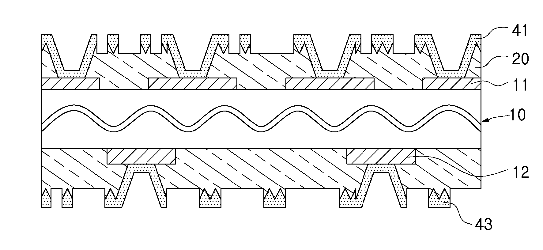
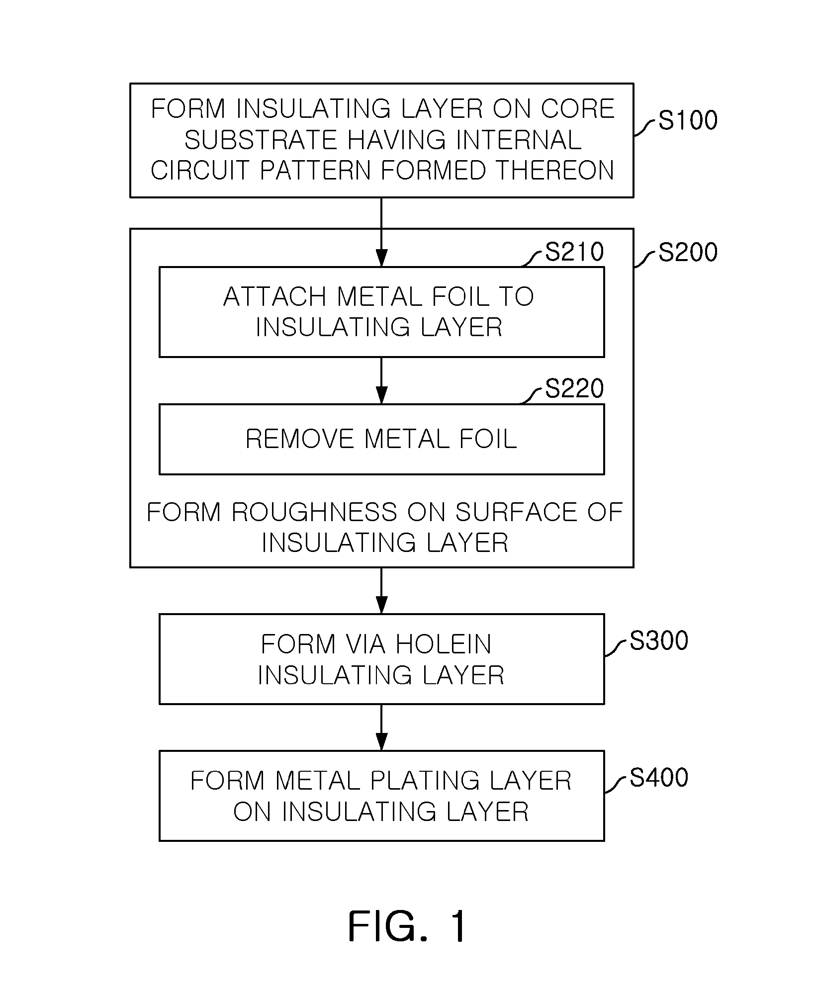
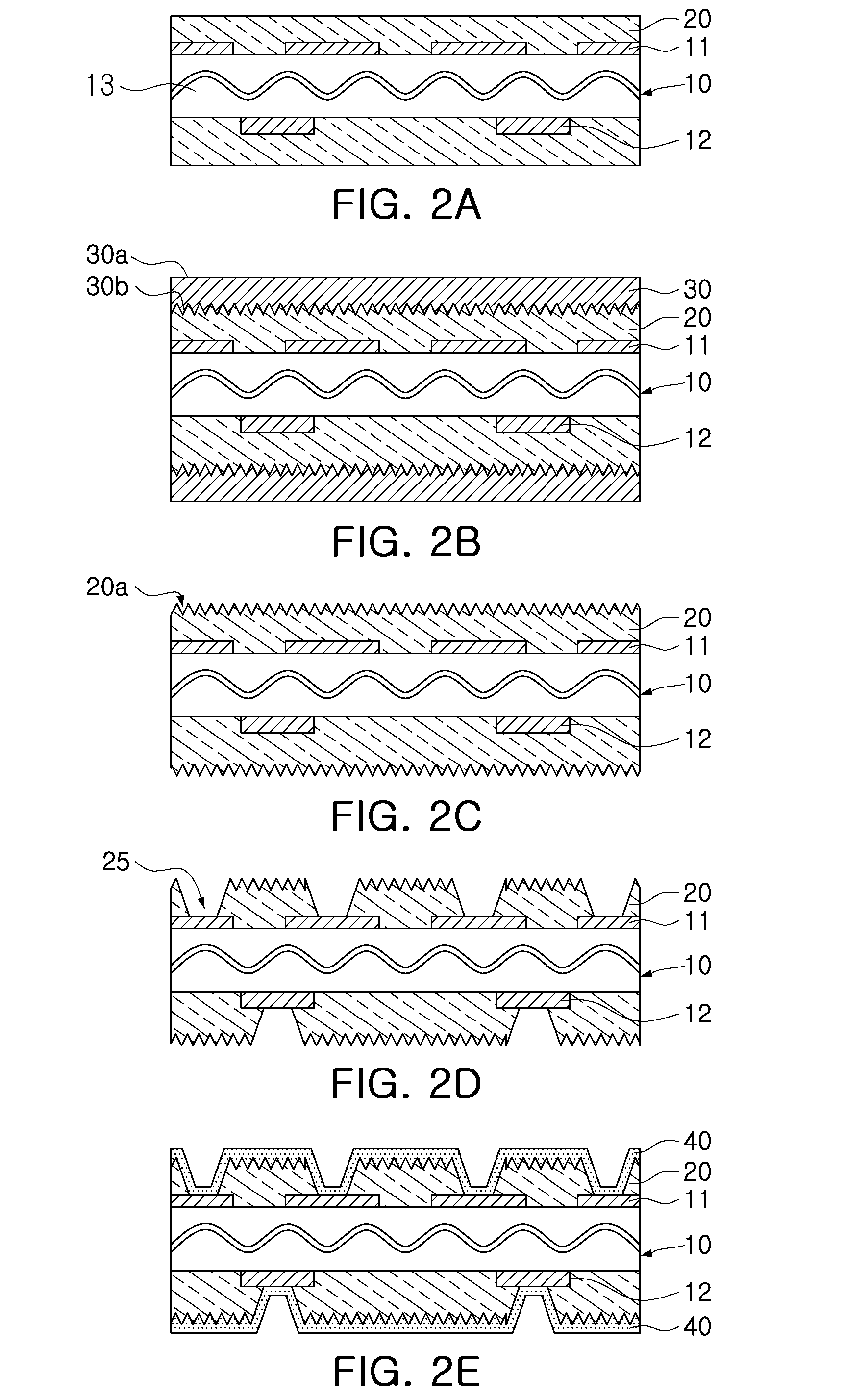
[0040]FIG. 1 is a flowchart showing a method of manufacturing a printed circuit board according to an exemplary embodiment of the present invention; FIG. 2...


PUM

PropertyMeasurementUnit
Raaaaaaaaaaa
Raaaaaaaaaaa
thicknessaaaaaaaaaa

Abstract

There are provided a printed circuit board and a method of manufacturing the same. The printed circuit board includes a first circuit pattern formed on a core substrate; an insulating layer stacked on the core substrate to cover the first circuit pattern and having a uniform surface roughness on a nano scale; a second circuit pattern formed on the insulating layer; and a via pattern electrically connecting the first circuit pattern to the second circuit pattern and penetrating through the insulating layer.

Description

CROSS-REFERENCE TO RELATED APPLICATIONS[0001]This application claims the priority of Korean Patent Application No. 10-2010-0115289 filed on Nov. 18, 2010, in the Korean Intellectual Property Office, the disclosure of which is incorporated herein by reference.BACKGROUND OF THE INVENTION[0002]1. Field of the Invention[0003]The present invention relates to a printed circuit board and a method of manufacturing the same, and more particularly, to a printed circuit board having a fine circuit pattern formed by having a uniform roughness formed on a surface of an insulating layer through a simple method and a method of manufacturing the same.[0004]2. Description of the Related Art[0005]Recently, in the field of electronics, a mounting technology using a high-density, high-resolution, and high-integration printed circuit board has been adopted when mounting components thereon in order to make electronic devices slim and compact. Such printed circuit boards are used in various roles, such as...

Claims


Application Information

Patent Timeline
Patent Type & Authority Applications(United States)
IPC IPC(8): H05K1/02H05K3/00
CPCH05K3/06H05K3/4602H05K3/4644Y10T29/49155H05K2201/0347H05K2203/1152H05K3/4652
Inventor JUNG, HYUNG MICHO, JAE CHOONLEE, CHOON KEUN
Owner SAMSUNG ELECTRO MECHANICS CO LTD
Why Eureka
Try Eureka