Porous lift-off layer for selective removal of deposited films

Inactive Publication Date: 2012-05-17
1366 TECH INC
View PDF7 Cites 3 Cited by
  • Summary
  • Abstract
  • Description
  • Claims
  • Application Information

AI Technical Summary

Benefits of technology

[0075]For semiconductor wafer processing, a porous lift off layer is used to facilitate removal of certain other applied materials, such as antireflection film coatings. A porous layer, composed of particles and porosities that are larger than the applied film layer, is provided in a region where no coating is desired. After the film has been applied over the porous layer and also other parts of the semiconductor where it is desired, the porous material is removed, which also results in removal of the overlying film that is not intended for those areas. The porous layer can be provided as a slurry, which is later dried to open up porosities, or a layer having fugitive particles within a field of some material, such as a heat degradable or liquid soluble particles, which disassociates from the field upon the application of heat or solvent. The film layer can be removed by etching away, by providing an etchant, which enters the film layer through porosities that have arisen due to the film not bridging the spaces between particles. The etchant flows throughout the porous layer, attacking the film from both of its surfaces. Particles may have diameters of, for instance, four to ten times the film thickness. Particles may be silica, alumina and other ceramics. Such porous layers can be used in depressions into which metallization is to be provided, to protect the depression from antireflective coating.

Problems solved by technology

However, some approaches to metallization cannot have such a reactive component and therefore the dielectric must be opened before the metallization.
After the coating film has been applied over the porous layer and also other parts of the semiconductor where it is desired, the porous material is removed, which also results in removal of the overlying film from areas where it is not desired.

Method used


Image

  • Porous lift-off layer for selective removal of deposited films
  • Porous lift-off layer for selective removal of deposited films
  • Porous lift-off layer for selective removal of deposited films

Examples


example

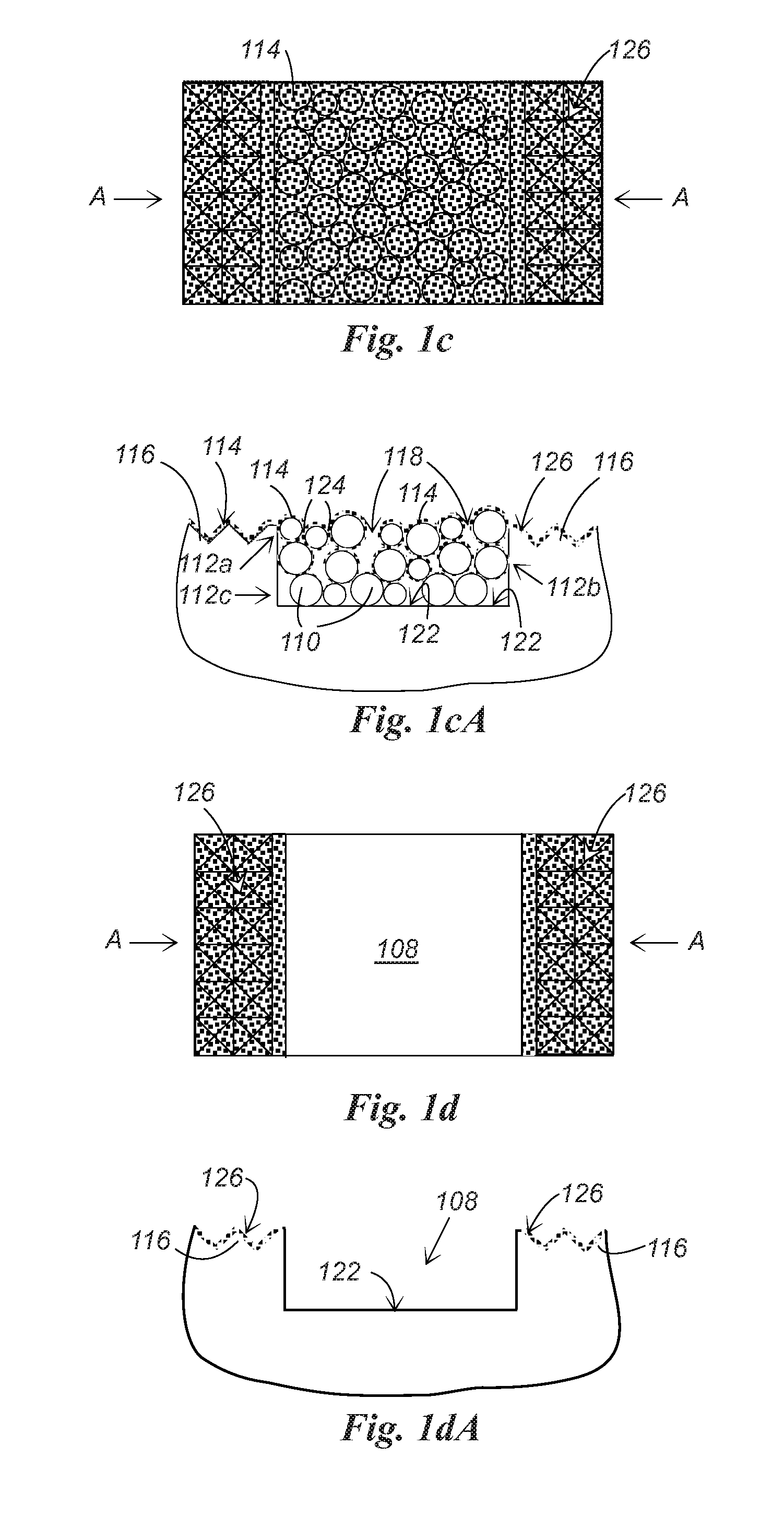
[0037]FIGS. 1a, 1b, 1c, 1d and 1e, and their respective cross-sections FIGS. 1aA, 1bA, 1cA, 1dA and 1eA show a method disclosed herein applied to blocking the deposition of a silicon nitride antireflection coating 114 (FIGS. 1c and 1cA) on the front 104 of a silicon solar cell 102. In this case, a slurry (not shown) of 1-2 micron diameter spherical silica powder particles 110 can be prepared in water with Polyethylenimine (PEI) as a dispersant. A typical slurry composition is approximately 1:1 water:silica by weight with 0.03 parts by weight of PEI as a dispersant. Many other polymeric dispersants are known in the art for dispersing silica, such as an ammonium salt of a polyelectrolyte, for example, as sold under the tradename Duramax 3005, from Rohm and Haas, of Philadelphia, Pa. Silica can also be dispersed electrostatically—by controlling the pH of the slurry. (Rather than silica, the powder in the slurry could be, alumina, silicon carbide, silicon nitride and other ceramic mater...


PUM


Abstract

A porous lift off layer facilitates removal of films from surfaces, such as semiconductors. A film is applied over a patterned porous layer, the layer comprising openings typically larger than the film thickness. The porous material and the film are then removed from areas where film is not intended. The porous layer can be provided as a slurry, dried to open porosities, or fugitive particles within a field, which disassociate upon the application of heat or solvent. The film can be removed by etchant that enters through porosities where the film does not bridge the spaces between solid portions, so that the etchant attacks both film surfaces

Description

RELATED DOCUMENTS[0001]Priority is hereby claimed to U.S. Provisional application Ser. No. 61 / 215,671, entitled POROUS LIFT-OFF LAYER FOR SELECTIVE REMOVAL OF DEPOSITED FILMS, in the names of Emanuel M. Sachs and Andrew M. Gabor, filed on May 8, 2009, which is hereby incorporated herein fully by reference.[0002]Certain processing schemes and architecture are disclosed in Patent Cooperation Treaty Application No. PCT / US2008 / 002058, entitled SOLAR CELL WITH TEXTURED SURFACES, filed Feb. 15, 2008, in the names of Emanuel M. Sachs and James F. Bredt and the Massachusetts Institute of Technology, designating the United States of America, and also claiming priority to two provisional United States applications, U.S. No. 60 / 901,511, filed Feb. 15, 2007, and U.S. No. 61 / 011,933, filed Jan. 23, 2007. All of the PCT application and the two US provisional applications are hereby incorporated fully herein by reference. The technology disclosed in these applications is referred to herein collect...

Claims


Application Information

Patent Timeline
IPC IPC(8): H01L31/18H01L21/302
CPCH01L31/022425H01L31/18H01L21/76802H01L31/02363Y02E10/50H01L31/04H01L31/0216
Inventor SACHS, EMANUEL M.GABOR, ANDREW M.
Owner 1366 TECH INC
Why Eureka
Try Eureka