Solid state light emitting device and method for making the same

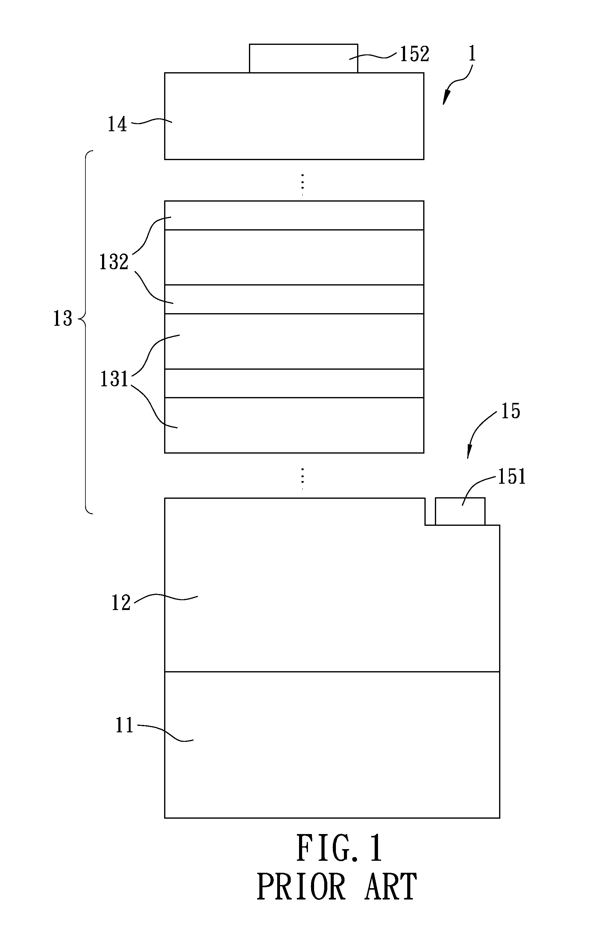
a light emitting device and solid-state technology, applied in the direction of semiconductor/solid-state device manufacturing, semiconductor devices, electrical devices, etc., can solve the problems of reducing the luminous efficiency recombination of carriers, and limited internal quantum efficiency of the active layer b>132/b> of the light emitting diode b>1/b>, so as to improve the internal quantum

Inactive Publication Date: 2012-05-10
LEXTAR ELECTRONICS CORP
View PDF2 Cites 3 Cited by
  • Summary
  • Abstract
  • Description
  • Claims
  • Application Information

AI Technical Summary

Benefits of technology

[0020]The advantage of the present invention is to provide a method for manufacturing a solid state light emitting device having quantum clusters that have similar sizes and shapes and regular distribution, thereby improving the internal quantum efficiency and light emission uniformity of the solid state light emitting device.

Problems solved by technology

However, the internal quantum efficiency of the active layers 132 of the light emitting diode 1 is limited and relatively low because the quantum well structures of the active layers 132 are a two-dimensional structure where the carriers are relatively free to move therein and thus may stay at various energy states.
Moreover, after manufacture, the dislocation densities of the n-type cladding layer 12, the light emitting unit 13, and the p-type cladding layer 14 are relatively high that may adversely influence the recombination of the carriers, thereby reducing the luminous efficiency of the light emitting diode 1.

Method used


Image

  • Solid state light emitting device and method for making the same
  • Solid state light emitting device and method for making the same
  • Solid state light emitting device and method for making the same

Examples


Embodiment Construction

[0031]Before the present invention is described in greater detail with reference to the accompanying preferred embodiments, it should be noted herein that like elements are denoted by the same reference numerals throughout the disclosure.

[0032]Unless otherwise defined, all technical and scientific terms used herein have the meaning commonly understood by a person skilled in the art to which this invention belongs. For clarity, as used herein, the term “quantum cluster” is a quasi-zero-dimensional semiconductor material, i.e., abound state of an electron and hole, are confined in all three spatial dimensions and may include a plurality of quantum dots.

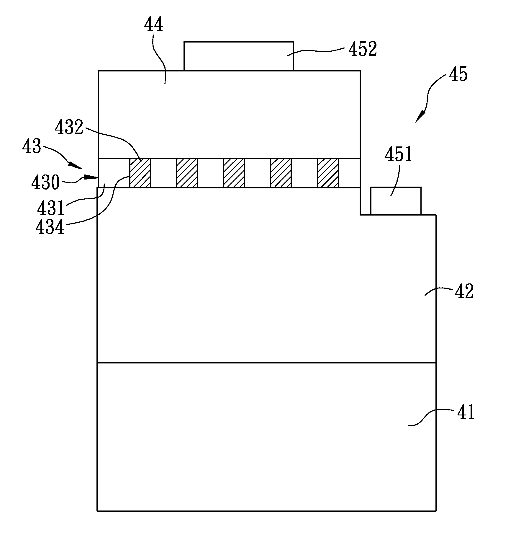
[0033]Referring to FIG. 4, the preferred embodiment of a solid state light emitting device of the present invention is a light emitting diode 4 that comprises a substrate 41, a first cladding layer 42, a second cladding layer 44, and a light emitting unit 43 disposed between the first and second cladding layers 42, 44, and an electrode ...


PUM


Abstract

A method for making a solid state light emitting device includes: (a) forming a first cladding layer on a substrate; (b) forming a matrix layer above the first cladding layer, the matrix layer having a top surface and being formed with a plurality of isolated spaces; (c) epitaxially forming a quantum cluster in each of the spaces such that the top surface of the matrix layer and top surfaces of the quantum clusters cooperatively define a coplanar surface, the quantum clusters cooperating with the matrix layer to form a light emitting layer; (d) forming a second cladding layer on the light emitting layer; and (e) forming an electrode unit electrically connected to the first and second cladding layers.

Description

CROSS-REFERENCE TO RELATED APPLICATION[0001]This application claims priority of Taiwanese application No. 099138489, filed on Nov. 9, 2010.BACKGROUND OF THE INVENTION[0002]1. Field of the Invention[0003]This invention relates to a solid state light emitting device and a method for making the same, more particularly to a solid state light emitting device including a structure of quantum clusters and a method for making the same.[0004]2. Description of the Related Art[0005]Solid state light emitting devices, especially light emitting diodes, have been widely applied in various fields, and, for example, can be used in a back module of a display, traffic signs, and lighting. Especially, a light emitting diode (LED) which is environmentally friendly and which has the advantage of energy conservation is quickly replacing traditional mercury lamps and incandescent lamps. In order to improve the applications of light emitting diodes, it is desired in the art to increase luminous brightness ...

Claims


Application Information

Patent Timeline
Patent Type & Authority Applications(United States)
IPC IPC(8): H01L33/04H01L33/00
CPCH01L33/007H01L33/08H01L33/06
Inventor CHEN, MING-SHENGLIANG, WEN-TENG
Owner LEXTAR ELECTRONICS CORP
Why Eureka
Try Eureka