
Semiconductor Devices and Methods of Manufacturing the Same

Active Publication Date: 2012-05-03
SAMSUNG ELECTRONICS CO LTD
View PDF18 Cites 227 Cited by
  • Summary
  • Abstract
  • Description
  • Claims
  • Application Information

AI Technical Summary

Benefits of technology

[0004]Some embodiments of the present invention provide semiconductor devices, which can facilitate a salicide process and can reduce or prevent damage to a gate due to misalignment.
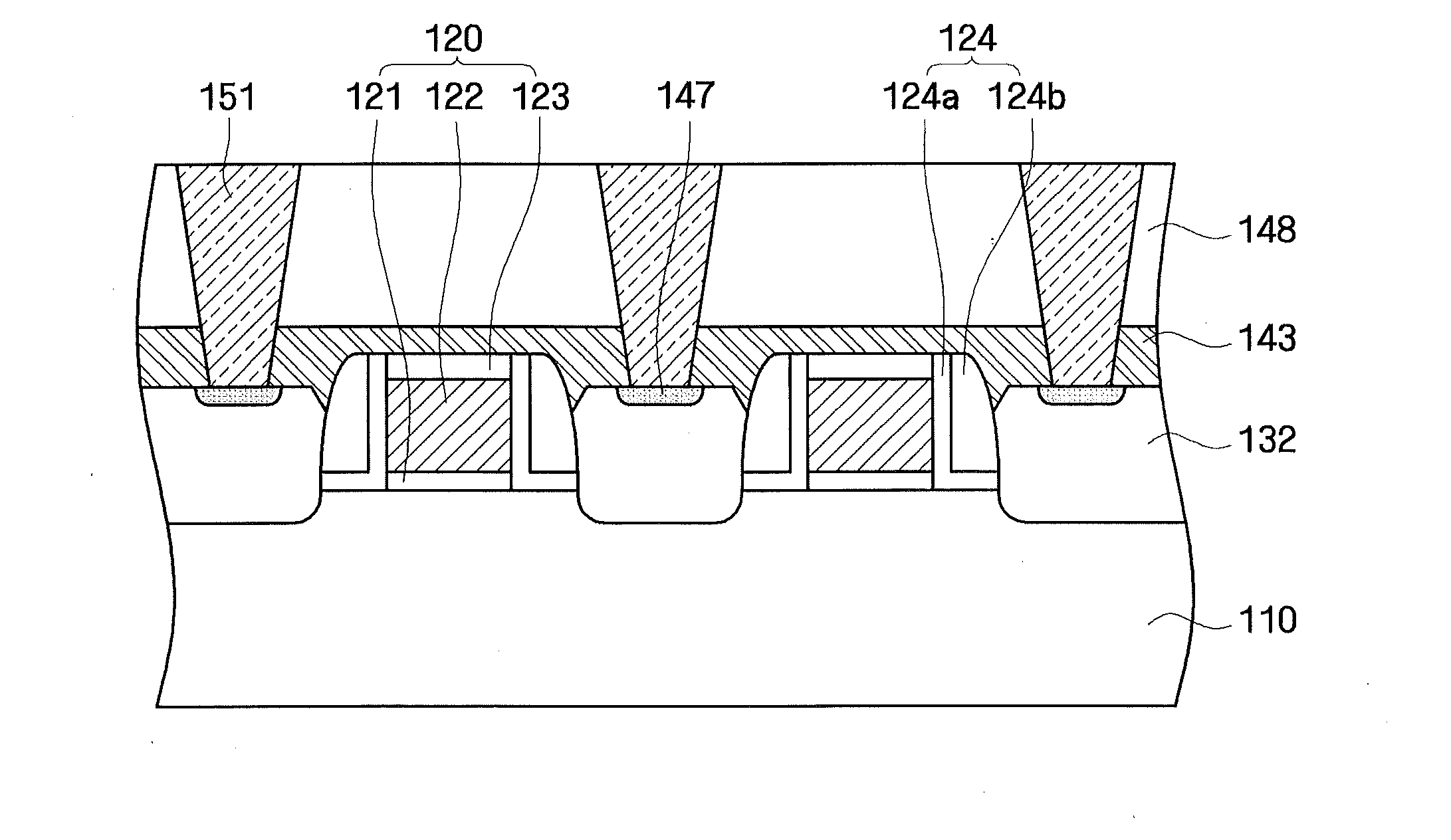
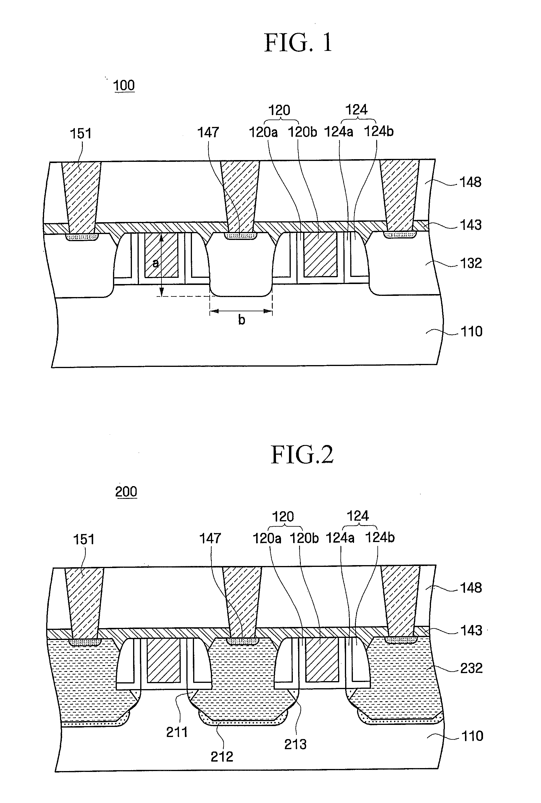
[0011]As described above, in the methods disclosed herein, since a silicide layer is formed on a source / drain region before forming a contact hole, a difficulty with deposition of a metal during a salicide process performed after forming the contact hole can be overcome.
[0012]In addition, in the methods disclosed herein, it is possible to reduce or prevent damage to a metal gate due to misalignment during a salicide process.
[0013]Further, since the semiconductor devices disclosed herein may have a relatively small step difference between a source / drain region and a gate, which reduces an aspect ratio of a contact hole, efficiency of subsequent processes may be increased.

Problems solved by technology

Accordingly, contact resistance and sheet resistance of the gate electrode tend to increase, which may undesirably lower the operating speed.
However, since a highly integrated semiconductor device may have a reduced gate line width compared to a height of the gate electrode, it may not be easy to deposit the metal material during the salicide process.
As such the metal gate may be damaged.
Further, the more highly integrated the semiconductor device, the smaller the manufacturing margin thereof.
Thus, in a case where misalignment occurs during the salicide process, a probability of the metal gate being damage may be increased.

Method used


Image

  • Semiconductor Devices and Methods of Manufacturing the Same
  • Semiconductor Devices and Methods of Manufacturing the Same
  • Semiconductor Devices and Methods of Manufacturing the Same

Examples


Embodiment Construction

[0021]Advantages and features of the present disclosure and methods of accomplishing the same may be understood more readily by reference to the following detailed description of preferred embodiments and the accompanying drawings. The present invention may, however, be embodied in many different forms and should not be construed as being limited to the embodiments set forth herein. Rather, these embodiments are provided so that this disclosure will be thorough and complete and will fully convey the concept of the invention to those skilled in the art, and the present invention will only be defined by the appended claims. In the drawings, the thickness of layers and regions are exaggerated for clarity.

[0022]It will be understood that when an element or layer is referred to as being “on,” or “connected to” another element or layer, it can be directly on or connected to the other element or layer or intervening elements or layers may be present. In contrast, when an element is referre...


PUM


Abstract

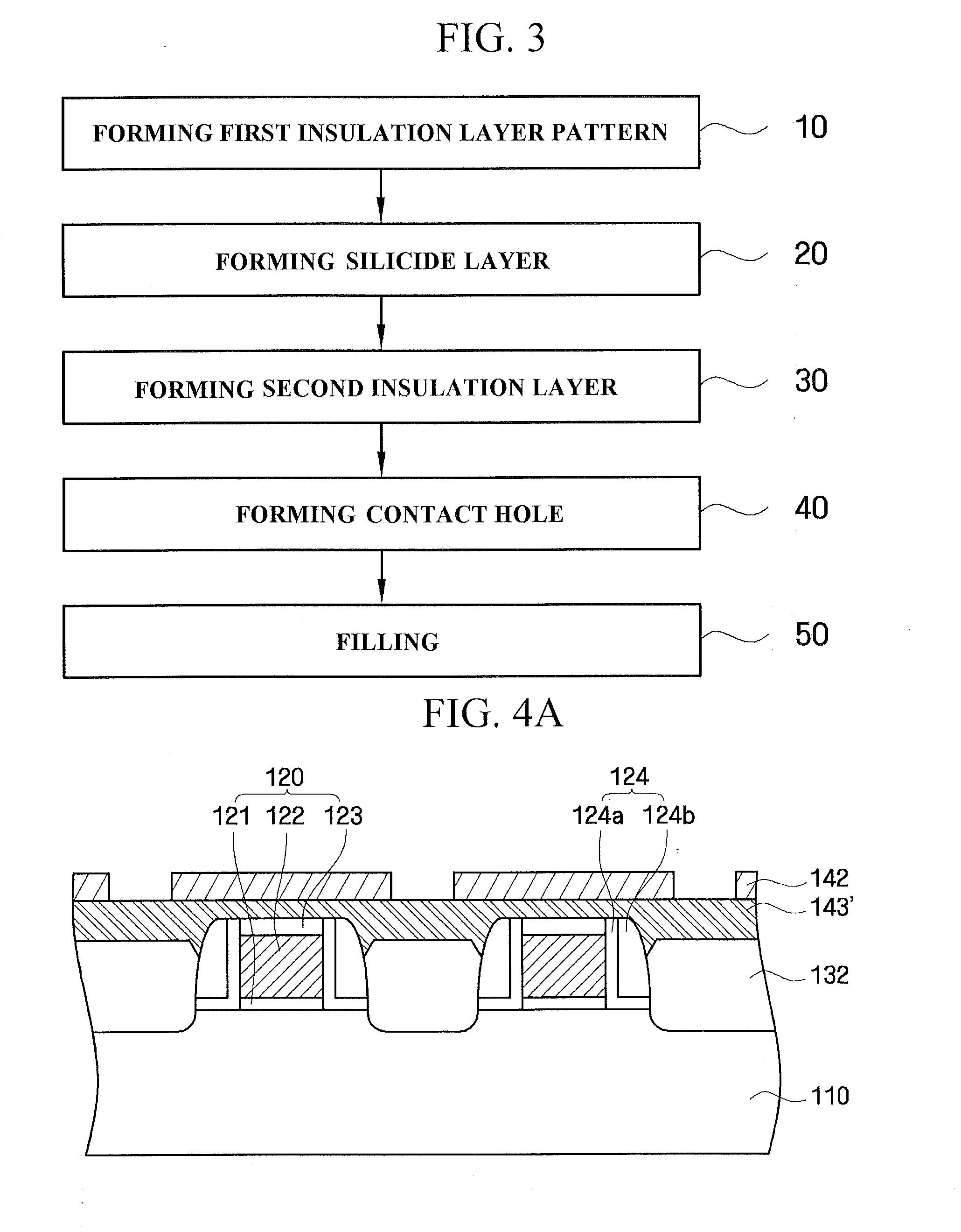
Provided are a semiconductor device, which can facilitate a salicide process and can prevent a gate from being damaged due to misalign, and a method of manufacturing of the semiconductor device. The method includes forming a first insulation layer pattern on a substrate having a gate pattern and a source / drain region formed at both sides of the gate pattern, the first insulation layer pattern having an exposed portion of the source / drain region, forming a silicide layer on the exposed source / drain region, forming a second insulation layer on the entire surface of the substrate to cover the first insulation layer pattern and the silicide layer, and forming a contact hole in the second insulation layer to expose the silicide layer.

Description

CROSS-REFERENCE TO RELATED APPLICATION[0001]This application claims priority from Korean Patent Application No. 10-2010-0108669 filed on Nov. 3, 2010 in the Korean Intellectual Property Office, and all the benefits accruing therefrom under 35 U.S.C. 119, the contents of which in its entirety are herein incorporated by reference.BACKGROUND[0002]A recent trend toward high integration of semiconductor devices uses a gate electrode of a memory device that occupies an increasingly smaller space. In this regard, the width and contact area of the gate electrode may be gradually reduced. Accordingly, contact resistance and sheet resistance of the gate electrode tend to increase, which may undesirably lower the operating speed. Therefore, a salicide (self-aligned silicide) process in which a metal gate is employed in order to reduce the resistance has been studied and developed.[0003]However, since a highly integrated semiconductor device may have a reduced gate line width compared to a heig...

Claims


Application Information

Patent Timeline
IPC IPC(8): H01L29/78H01L21/336
CPCH01L21/28518H01L21/76802H01L29/41775H01L29/495H01L29/4966H01L29/7848H01L29/66545H01L29/6659H01L29/66628H01L29/66636H01L29/7834H01L29/665H01L29/4175H01L29/7845
Inventor PARK, SANG-JINEYOON, BO-UNHAN, JEONG-NAMSONG, MYUNG-GEUN
Owner SAMSUNG ELECTRONICS CO LTD
Learn More