
P-pixel CMOS imagers using ultra-thin silicon on insulator substrates (UTSOI)

Inactive Publication Date: 2012-05-03
SRI INTERNATIONAL
View PDF4 Cites 12 Cited by
  • Summary
  • Abstract
  • Description
  • Claims
  • Application Information

AI Technical Summary

Benefits of technology

[0008]The above-described problems are addressed and a technical solution achieved in the art by providing an improved readout circuit for a CMOS image sensor, comprising: a semiconductor substrate having a surface; an epitaxial layer grown on the surface with a net n-type dopant concentration profile, the profile having a maximum value of net n-type doping concentration proximal to the surface in one of the semiconductor substrate and the epitaxial layer and which decreases monotonically with increasing distance from the maximum value within one of the semiconductor

Problems solved by technology

When a CCD imager is illuminated on the front side, absorption of incident light by the electronic circuitry reduces quantum efficiency.
As an alternative, CCDs may be illuminated from the back side; however, back side illumination produces other problems.
Therefore, for good blue and ultraviolet response, the substrate must be extremely thin in order to have acceptable charge spreading (crosstalk), resulting in a very fragile and expensive structure.

Method used


Image

  • P-pixel CMOS imagers using ultra-thin silicon on insulator substrates (UTSOI)
  • P-pixel CMOS imagers using ultra-thin silicon on insulator substrates (UTSOI)
  • P-pixel CMOS imagers using ultra-thin silicon on insulator substrates (UTSOI)

Examples


Embodiment Construction

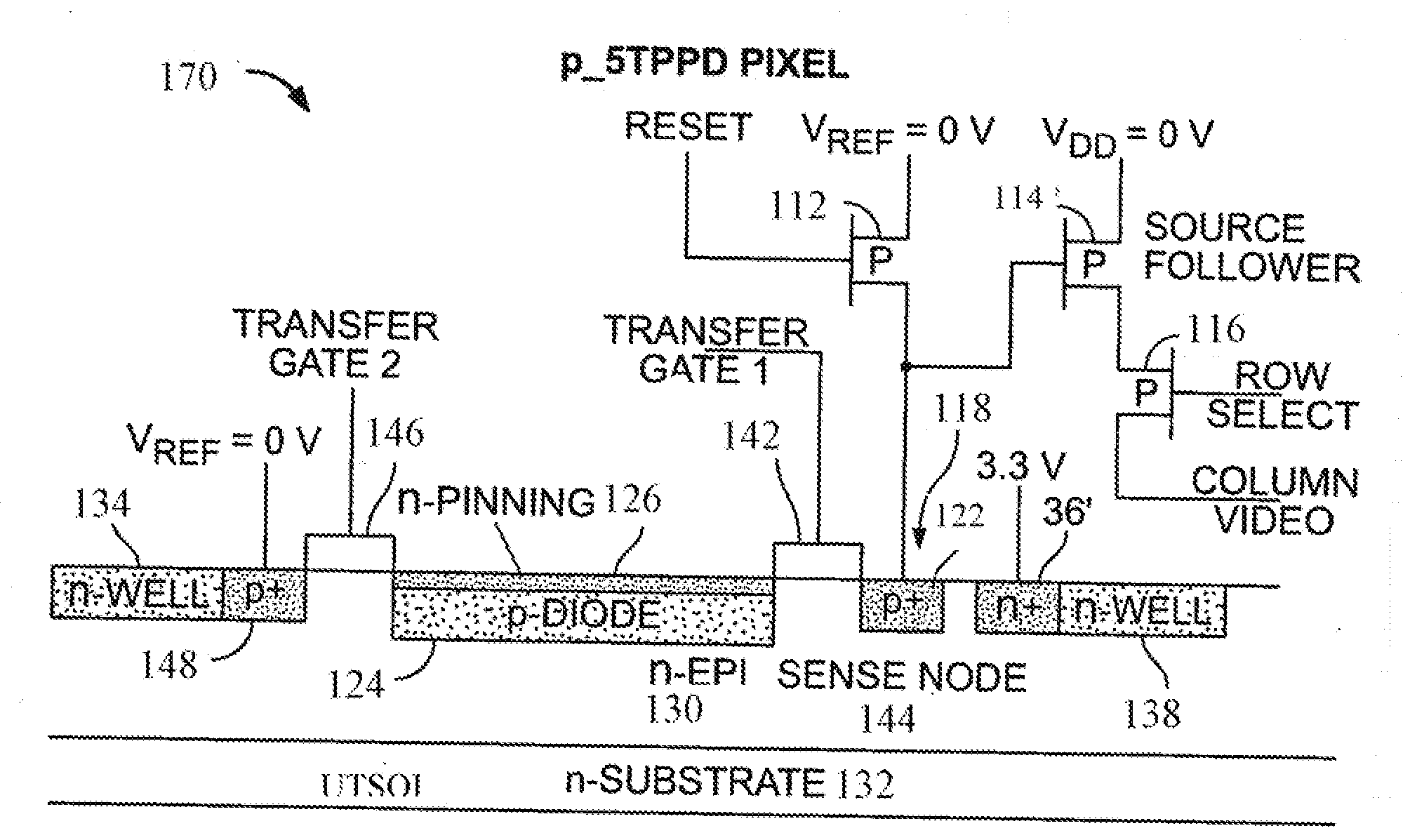
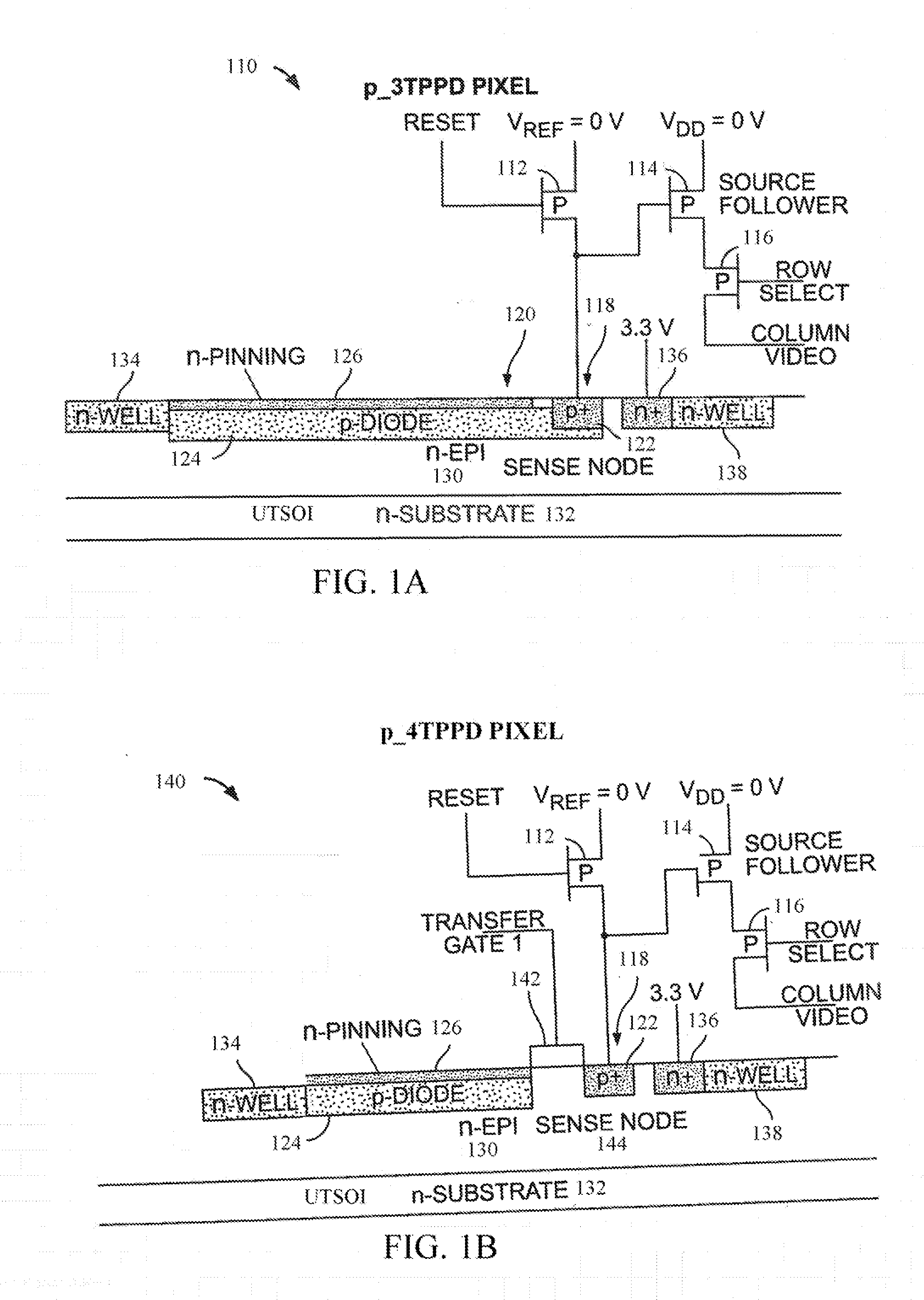
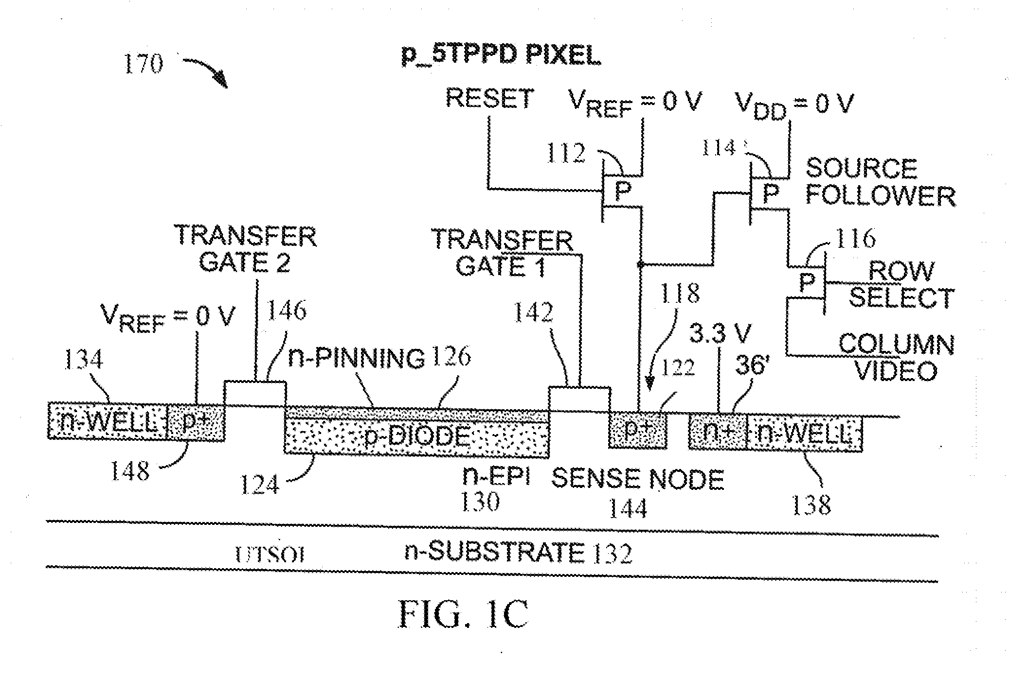
[0023]FIGS. 1A, 1B, and 1C are cross-sectional views of a p-type CMOS 3T pixel 110 (for three-transistor pixel), a 4T pixel 140 (for 3-transistor plus 1-transfer gate pixel), and a 5T pixel 170 (for 3-transistor plus 2-transfer gate pixel), respectively, according to an embodiment of the present invention. The p-type CMOS pixels are hereinafter designated as p—3TPPD, p—4TPPD and p—5TPPD pixels, 110, 140, 170, respectively (collectively referred to as p_pixels). The p—3TPPD pixel 110 includes three PMOS transistors 112, 114, 116 standing for a reset transistor 112, a source follower transistor 114 and a row transistor 116. The reset transistor 112 is electrically connected to a sense node 118. The sense node 118 is formed of a p+ contact 122 and a pinned photodiode 120. The pinned photodiode 120 includes a thin n-type pinning layer 126 overlying a custom p-diode implant 124, that in turn, overlies and forms a depletion region with an n-epitaxial layer 130. An ultra-thin silicon-on-in...


PUM


Abstract

A CMOS image sensor is disclosed. The CMOS image sensor includes a semiconductor substrate having a surface. An epitaxial layer is grown on the surface. A p-type CMOS pixel formed substantially in the epitaxial layer. In one version of the CMOS image sensor, there exists a net n-type dopant concentration profile in the semiconductor substrate and the epitaxial layer which has a maximum value at a predetermined distance from the surface and which decreases monotonically on both sides of the profile from the maximum value within the semiconductor substrate and the epitaxial layer. In another version of the CMOS image sensor, there exists a net n-type dopant concentration profile in the semiconductor substrate and the epitaxial layer which has a maximum value at the surface and which decreases monotonically with increasing distance from the surface within the semiconductor substrate and the epitaxial layer.

Description

CROSS-REFERENCES TO RELATED APPLICATIONS[0001]This application claims the benefit of U.S. provisional patent application No. 61 / 407,993 filed Oct. 29, 2010, the disclosure of which is incorporated herein by reference in its entirety.FIELD OF THE INVENTION[0002]The field of invention is semiconductor device fabrication and device structure. More specifically, the field is fabrication and structure of PMOS semiconductor imaging devices that employ ultra thin silicon on insulator (UTSOI) substrates.BACKGROUND OF THE INVENTION[0003]CMOS image sensors first came to the fore in relatively low-performance applications where shuttering was not required, scene dynamic range was low, and moderate to high noise levels could be tolerated. A CMOS sensor technology enabling a higher level of integration of an image array with associated processing circuits would be beneficial to many digital applications such as, for example, in cameras, scanners, machine vision systems, vehicle navigation system...

Claims


Application Information

Patent Timeline
IPC IPC(8): H01L27/146
CPCH01L21/84H01L27/14603H01L27/14674H01L27/1464H01L27/14643H01L27/14609
Inventor JANESICK, JAMES ROBERTLEVINE, PETER ALANTOWER, JOHN ROBERTSON
Owner SRI INTERNATIONAL
Learn More