
Carbazole Compound, Material for Light-Emitting Element, Organic Semiconductor Material, Light-Emitting Element

a technology of organic semiconductor materials and compounds, applied in the direction of discharge tubes/lamp details, organic chemistry, discharge tubes luminescnet screens, etc., can solve the problems of limited material in contact with phosphorescent light-emitting materials, limited structure to be selected, etc., to achieve good carrier-transport properties, good emission efficiency, and low driving voltage

Active Publication Date: 2012-04-19
SEMICON ENERGY LAB CO LTD
View PDF8 Cites 23 Cited by
  • Summary
  • Abstract
  • Description
  • Claims
  • Application Information

AI Technical Summary

Benefits of technology

[0010]It is an object of one embodiment of the present invention to provide a novel carbazole compound that can be used as a transport layer, a host material, or a light-emitting material in a light-emitting element.
[0014]It is an object of another embodiment of the present invention to provide a light-emitting element with high emission efficiency.
[0016]It is an object of another embodiment of the present invention to provide a light-emitting element with long lifetime.
[0031]A carbazole compound of the present invention having the above-described structure can be synthesized easily, and thus is a more preferable carbazole compound.
[0064]The carbazole compound of the present invention having the above-described structure can be synthesized easily, and thus a light-emitting element including a carbazole compound having a more preferable structure can be provided.
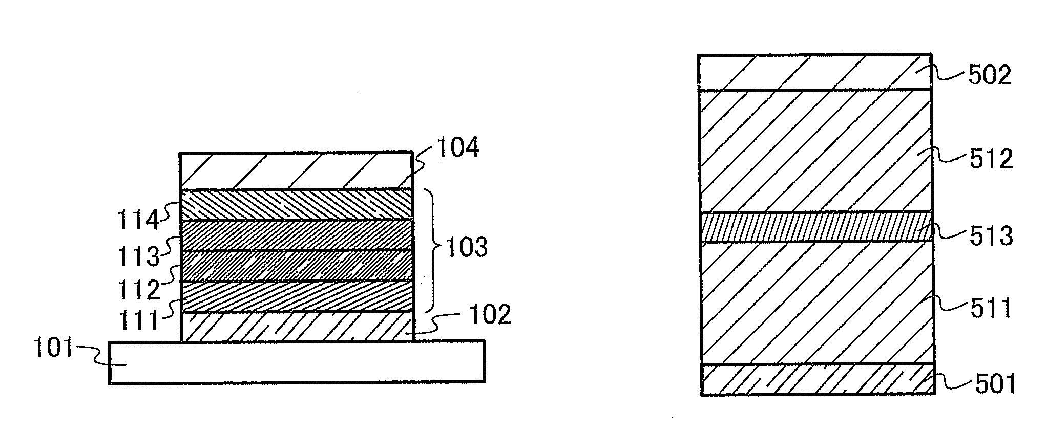
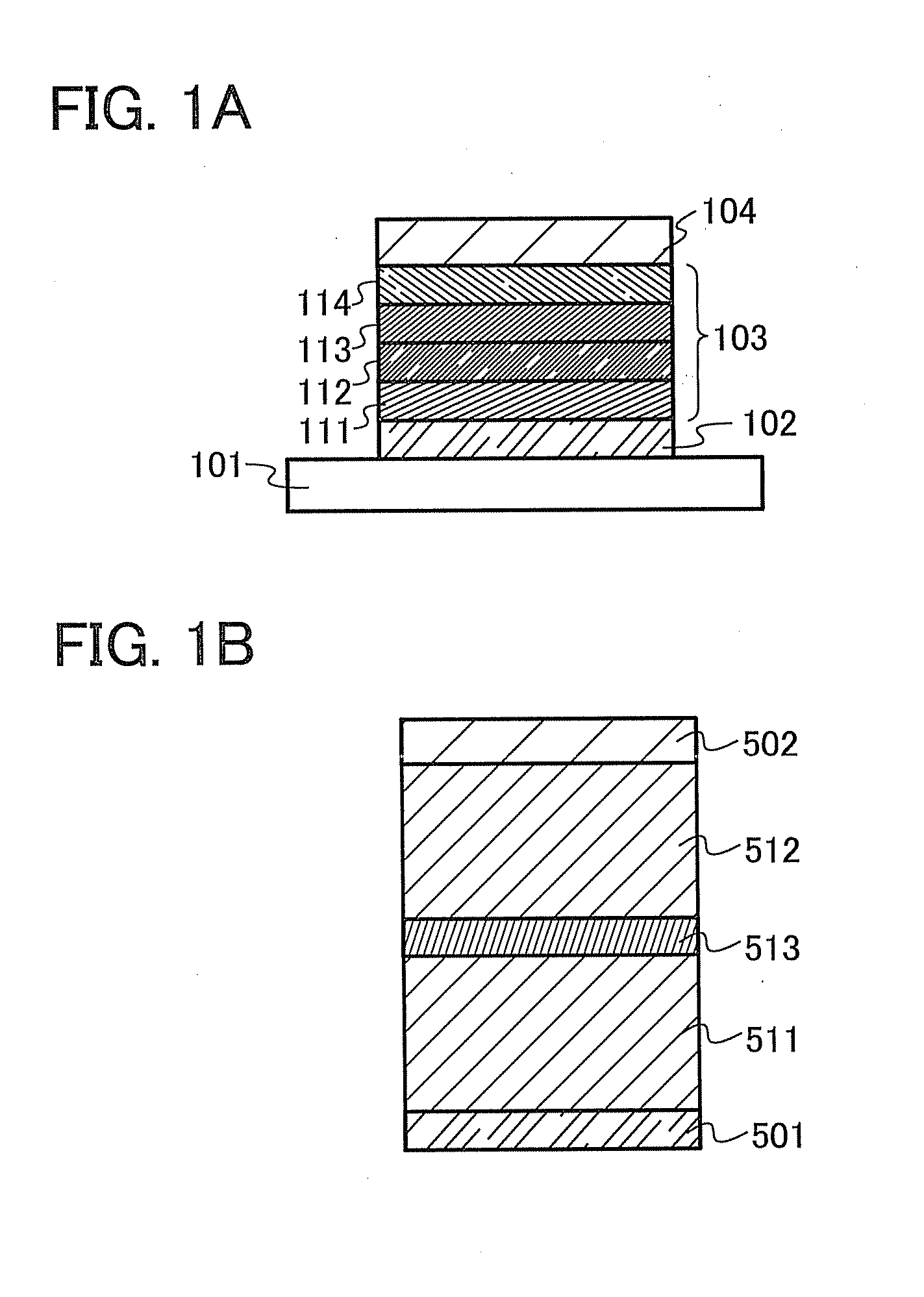
[0085]A light-emitting element including, as a part of a functional layer in a layer containing an organic compound between electrodes, the carbazole compound having a wide band gap and / or a T1 level can be a light-emitting element with a good emission efficiency. Further, a light-emitting element including, as a part of a functional layer in a layer containing an organic compound between electrodes, the carbazole compound having a good carrier-transport property can be a light-emitting element driven with low driving voltage. Furthermore, a light-emitting element including, as a part of a functional layer in a layer containing an organic compound between electrodes, the carbazole compound can be a light-emitting element with long lifetime.

Problems solved by technology

However, when a material with a low molecular weight is used, a structure to be selected is limited.
In particular, since a T1 level is lower than an S1 level, a material in contact with a phosphorescent light-emitting material is limited.

Method used


Image

  • Carbazole Compound, Material for Light-Emitting Element, Organic Semiconductor Material, Light-Emitting Element
  • Carbazole Compound, Material for Light-Emitting Element, Organic Semiconductor Material, Light-Emitting Element
  • Carbazole Compound, Material for Light-Emitting Element, Organic Semiconductor Material, Light-Emitting Element

Examples


embodiment 1

[0145]A carbazole compound in this embodiment is a carbazole compound in which the 4-position of a dibenzothiophene skeleton or a dibenzofuran skeleton is bonded to the 2- or 3-position of a carbazole skeleton directly or via an arylene group. Note that any of a phenyl group, a biphenyl group, and a naphthyl group is bonded to nitrogen of the carbazole skeleton. The carbazole compound has a good carrier-transport property, a good film quality, a wide band gap, and / or a high T1 level. For that reason, the carbazole compound can be used suitably as a material of a light-emitting element or an organic semiconductor material.

[0146]Dibenzothiophene or dibenzofuran bonded to the carbazole may have a substituent, and when dibenzothiophene or dibenzofuran has a substituent, the substituent can be an alkyl group having 1 to 6 carbon atoms or an aryl group having 6 to 13 carbon atoms.

[0147]In addition, when the carbazole has another substituent, the substitution site is a carbon atom at 6- or...

embodiment 2

[0185]As a synthesis method of the carbazole compound described in Embodiment 1, a variety of reactions can be applied. For example, by synthesis reactions represented by the following synthesis method 1 to synthesis method 4, a carbazole compound can be synthesized. Note that for the symbols (α1, Ar1, Ar2, Ar3, n, α, β, γ, δ), which are not described here, the description of the general formula (G1) described above can be referred to.

[Synthesis Method 1]

[0186]First, as shown in the reaction scheme (S-1), a carbazole compound (a1) and an aryl halide compound (a2) are coupled with each other, so that the carbazole compound (G1) described in Embodiment 1 can be synthesized.

[0187]Further, X1 is a halogen. X1 preferably is bromine, more preferably iodine, because they have high reactivity.

[0188]Note that a variety of reaction conditions can be employed for the coupling reaction between an aryl compound having a halogen group and the 9-position of the carbazole in the reaction scheme (S-...

embodiment 3

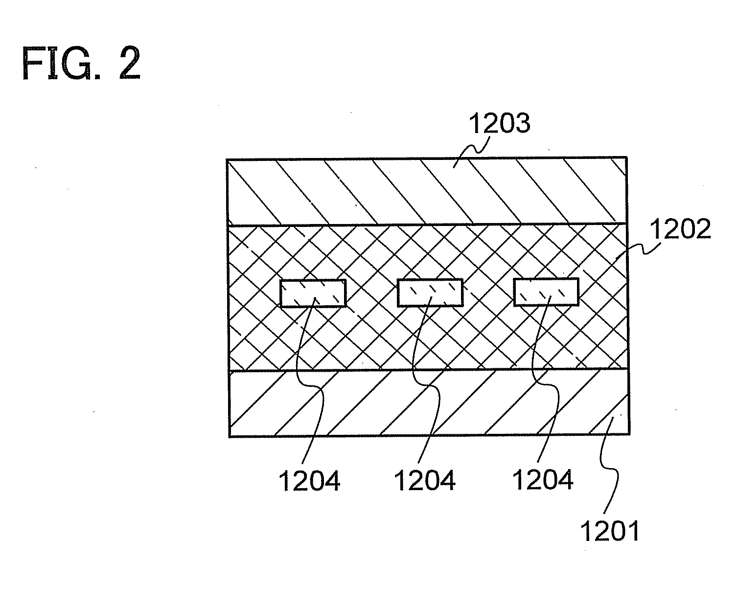
[0212]This embodiment shows an example in which the carbazole compound of Embodiment 1 is used for an active layer of a vertical transistor (SIT), which is a kind of an organic semiconductor element.

[0213]The element has a structure in which a thin-film active layer 1202 containing any one of the carbazole compounds described in Embodiment 1 is interposed between a source electrode 1201 and a drain electrode 1203, and gate electrodes 1204 are embedded in the thin-film active layer 1202, as illustrated in FIG. 2. The gate electrodes 1204 are each electrically connected to a unit to apply a gate voltage, and the source electrode 1201 and the drain electrode 1203 are electrically connected to a unit to control a voltage between the source and the drain.

[0214]In such an element structure, when a voltage is applied between the source and the drain without a gate voltage applied, a current flows (an ON state). Then, when a gate voltage is applied at this time, a depletion layer is generat...


PUM

PropertyMeasurementUnit
excitation energyaaaaaaaaaa
band gapaaaaaaaaaa

Abstract

To provide a novel carbazole compound that has an excellent carrier-transport property and can be used for a transport layer or as a host material in a light-emitting element. Further, to provide an organic semiconductor material and a material for a light-emitting element using the carbazole compound. A carbazole compound in which the 4-position of a dibenzothiophene skeleton or a dibenzofuran skeleton is substituted with the 2- or 3-position of a carbazole skeleton directly or via an arylene group can be synthesized. The carbazole compound is found to have a suitable carrier-transport property, a good film quality, and be used suitably as a material of a light-emitting element and an organic semicondcutor material. Note that nitrogen of the carbazole skeleton is substituted with any of a phenyl group, a biphenyl group, and a naphthyl group.

Description

BACKGROUND OF THE INVENTION[0001]1. Field of the Invention[0002]The present invention relates to carbazole compounds. Further, the present invention relates to materials for light-emitting elements, organic semiconductor materials, and light-emitting elements using the carbazole compounds.[0003]2. Description of the Related Art[0004]A display device using a light-emitting element (organic EL element) in which an organic compound is used as a light-emitting substance has been developed rapidly as a next generation lighting device or display device because it has advantages that such a light-emitting element can be formed to be thin and lightweight, has very high response speed for input signals, and has low power consumption.[0005]In an organic EL element, when voltage is applied between a pair of electrodes with a light-emitting layer interposed therebetween, electrons and holes injected from the electrodes are recombined to form an excited state, and when the excited state returns ...

Claims


Application Information

Patent Timeline
Patent Type & Authority Applications(United States)
IPC IPC(8): H05B33/14C07D405/14C07D405/10C07D409/14C07D409/10H10K99/00
CPCC07D405/04H01L51/5278C07D405/14C07D409/04C07D409/10C07D409/14C09K11/06C09K2211/1007C09K2211/1011C09K2211/1029C09K2211/1092H01L51/0054H01L51/0058H01L51/006H01L51/0072H01L51/0074H01L51/5012H01L51/5016H01L51/5048C07D405/10H10K85/622H10K85/626H10K85/633H10K85/6576H10K85/6572H10K50/11H10K2101/10H10K50/14H10K50/19
Inventor OSAKA, HARUESHITAGAKI, SATOKONOWATARI, HIROMIOHSAWA, NOBUHARU
Owner SEMICON ENERGY LAB CO LTD
Learn More