
Data security for dynamic random access memory using body bias to clear data at power-up

a dynamic random access memory and data security technology, applied in static storage, digital storage, instruments, etc., can solve the problems of increasing the leakage time, increasing the security of traditional dram chips such as those used for memory in computer laptops and other electronic devices, and being particularly vulnerable to data theft in dram memory. , to achieve the effect of increasing the body voltage of cells, reducing the threshold voltage of nfet transistors, and increasing data security

Active Publication Date: 2012-04-12
MARVELL ASIA PTE LTD
View PDF4 Cites 4 Cited by
  • Summary
  • Abstract
  • Description
  • Claims
  • Application Information

AI Technical Summary

Benefits of technology

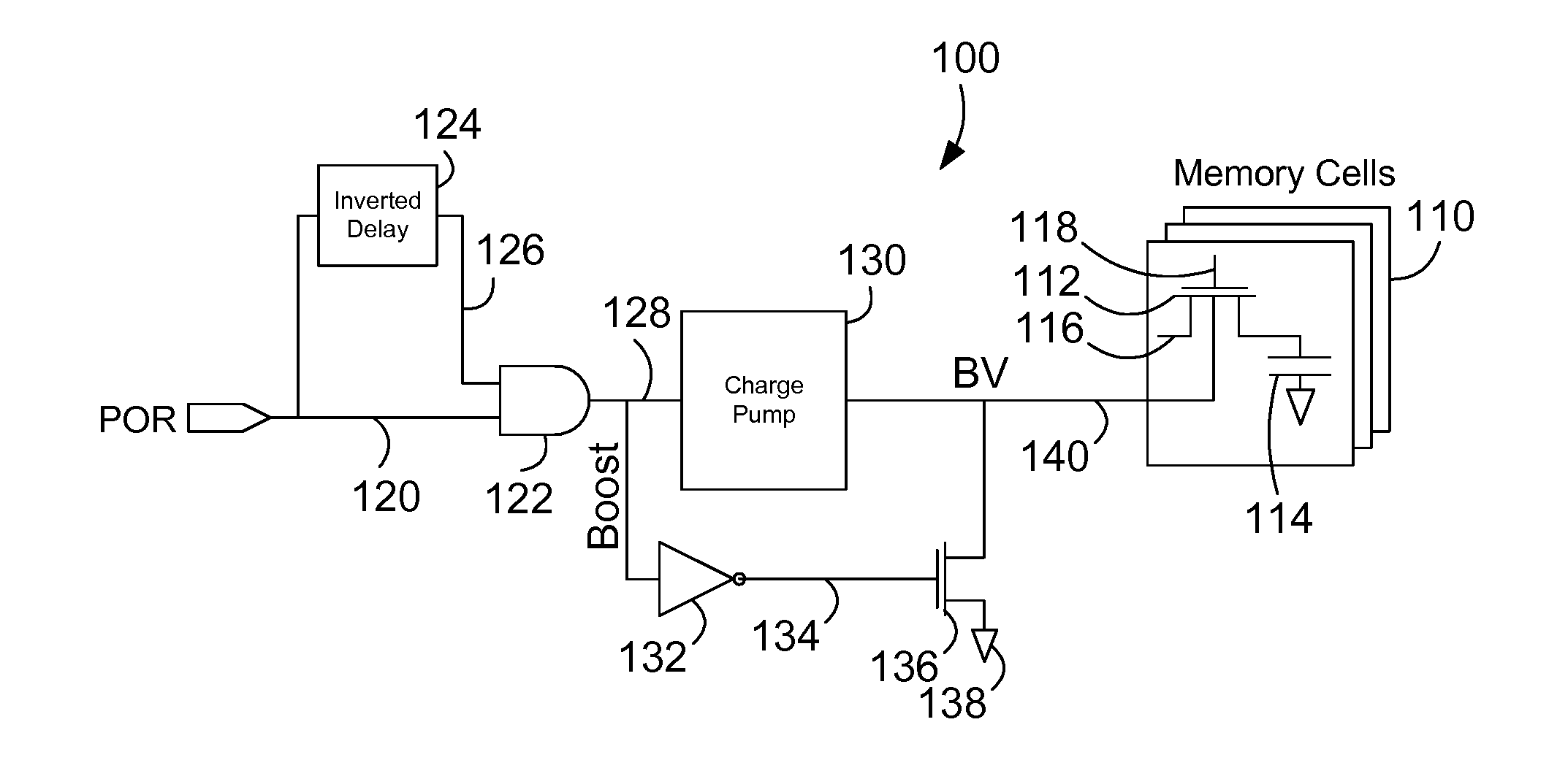
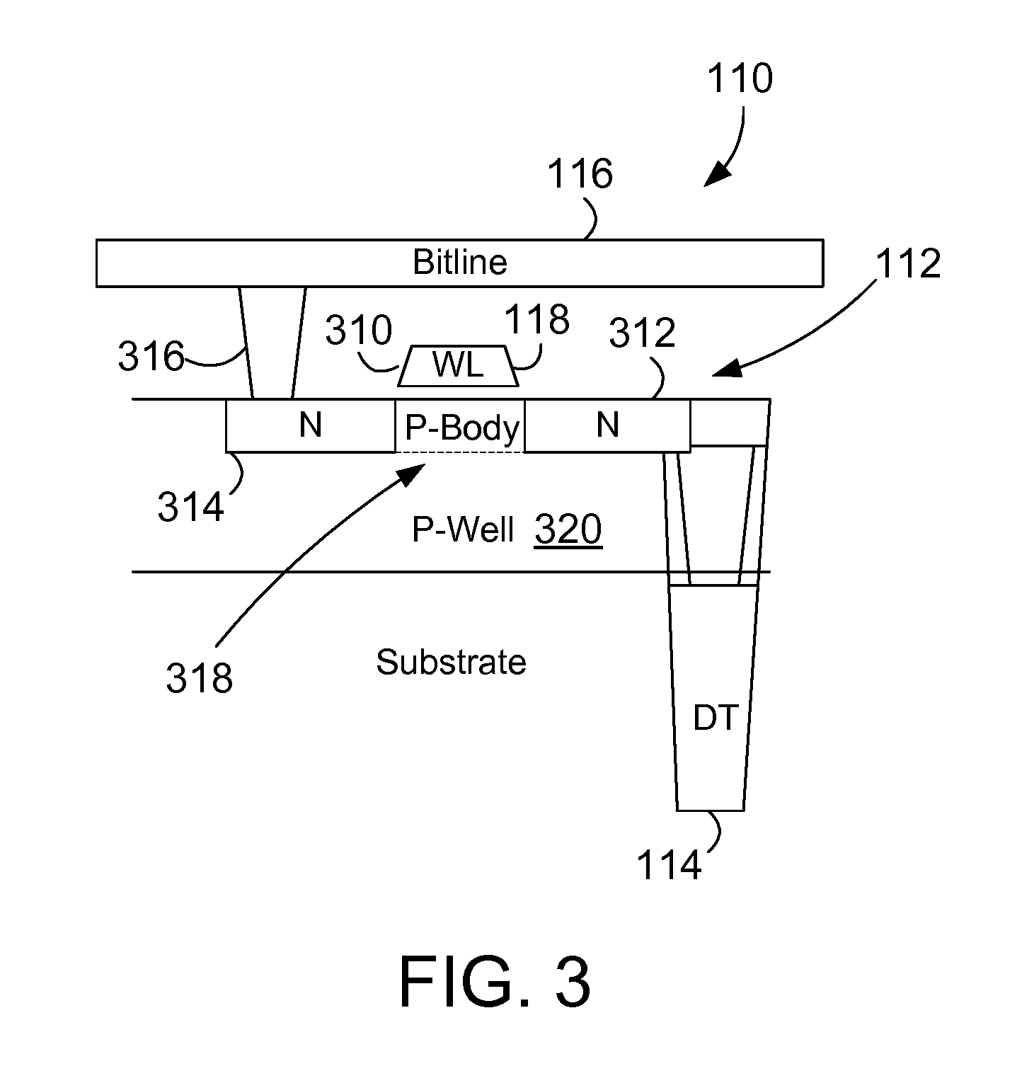
[0006]The disclosure is directed to a circuit and method for erasing at power-up all data stored in a DRAM chip for increased data security. All the DRAM memory cells are erased by turning on the transistors for the DRAM storage cells simultaneously by increasing the body voltage of cells. In the example circuit, the body voltage is increased by a charge pump controlled by a power-on-reset (POR) signal applying a voltage to the p-well of the memory cells. The added voltage to the p-well lowers the threshold voltage of the NFET transistor of the memory cell, such that the transistor of the memory cell will turn on. With all the devices turned on, the data stored in the memory cells is erased as the voltage of all the cells connected to a common bitline coalesce to a single value.

Problems solved by technology

It has been shown that traditional DRAM chips such as those used for memory in computer laptops and other electronic devices have security issues.
In addition, the leak off time can be dramatically increased by chilling the DRAM device.
Computer laptops or other portable computer devices are particularly vulnerable to theft of data in DRAM memory.

Method used


Image

  • Data security for dynamic random access memory using body bias to clear data at power-up
  • Data security for dynamic random access memory using body bias to clear data at power-up
  • Data security for dynamic random access memory using body bias to clear data at power-up

Examples


Embodiment Construction

[0013]Described herein is an apparatus and method for erasing at power-up all data stored in a DRAM chip for increased data security. All the DRAM memory cells are erased by turning on the transistors for the DRAM storage cells simultaneously by increasing the body voltage of cells. In the example circuit, the body voltage is increased by a charge pump controlled by a power-on-reset (POR) signal applying a voltage to the p-well of the memory cells. The added voltage to the p-well lowers the threshold voltage of the NFET transistor of the memory cell, such that the transistor will turn on. With all the devices turned on, the data stored in the memory cells is erased as the voltage of all the cells connected to a common bitline coalesce to a single value.

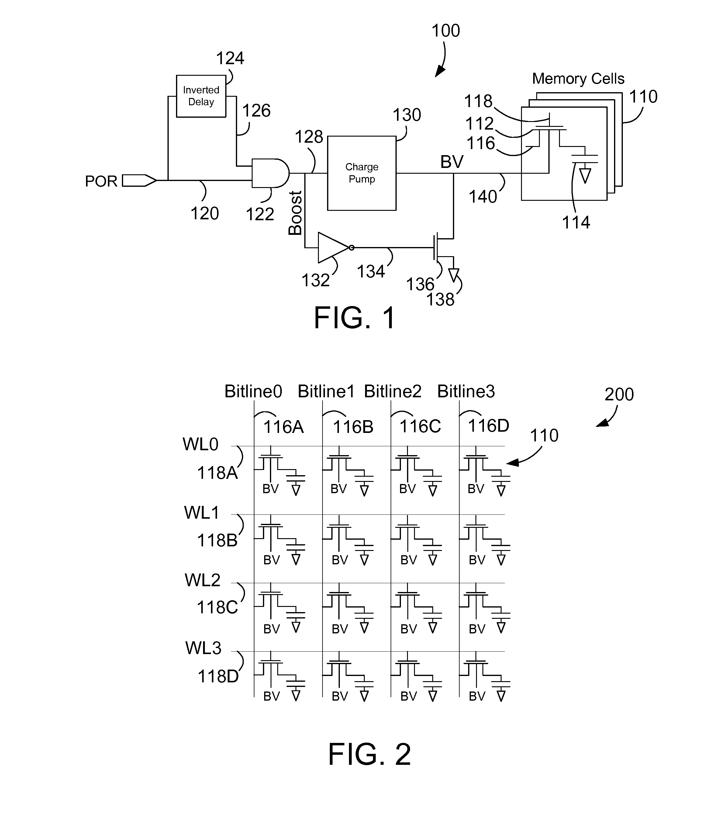
[0014]FIG. 1 is an example circuit 100 for erasing DRAM memory cells 110 at power up for increased security of DRAM memory. A DRAM memory is typically made of many memory cells 110 with a cell for each bit of the memory. The DRAM memo...


PUM


Abstract

A circuit and method erase at power-up all data stored in a DRAM chip for increased data security. All the DRAM memory cells are erased by turning on the transistors for the DRAM storage cells simultaneously by increasing the body voltage of cells. In the example circuit, the body voltage is increased by a charge pump controlled by a power-on-reset (POR) signal applying a voltage to the p-well of the memory cells. The added voltage to the p-well lowers the threshold voltage of the cell, such that the NFET transistor of the memory cell will turn on. With all the devices turned on, the data stored in the memory cells is erased as the voltage of all the cells connected to a common bitline coalesce to a single value.

Description

BACKGROUND[0001]1. Technical Field[0002]This disclosure generally relates to data security and dynamic random access memory (DRAM), and more specifically relates to providing data security for data stored in a DRAM by using body bias to clear any persistent data on power up of the DRAM chip.[0003]2. Background Art[0004]It has been shown that traditional DRAM chips such as those used for memory in computer laptops and other electronic devices have security issues. While it is commonly thought that the data on a DRAM chip is no longer available after powering down the chip, actually the data on the chip is persistent such that the data may still be available after power is turned off. The data, stored as a charge on a capacitor, is still available because the charge on the individual DRAM capacitors leaks off very slowly. In addition, the leak off time can be dramatically increased by chilling the DRAM device. An intruder could possibly obtain access to secure information in the DRAM....

Claims


Application Information

Patent Timeline
Patent Type & Authority Applications(United States)
IPC IPC(8): G11C11/24G11C7/00
CPCG11C5/145G11C7/20G11C11/4078G11C11/4072G11C7/24
Inventor BEHRENDS, DERICK GARDNERCHRISTENSEN, TODD ALANHEBIG, TRAVIS REYNOLDLAUNSBACH, MICHAELNELSON, DANIEL MARK
Owner MARVELL ASIA PTE LTD
Learn More