
Fet structures with trench implantation to improve back channel leakage and body resistance

a back channel leakage and body resistance technology, applied in the field of improving the parasitic leakage of mosfet (metal oxide semiconductor field effect transistor) structure of semiconductors, can solve the problems of low body resistance and interference with threshold voltage, affecting semiconductor reliability

Active Publication Date: 2012-04-12
IBM CORP
View PDF3 Cites 20 Cited by
  • Summary
  • Abstract
  • Description
  • Claims
  • Application Information

AI Technical Summary

Benefits of technology

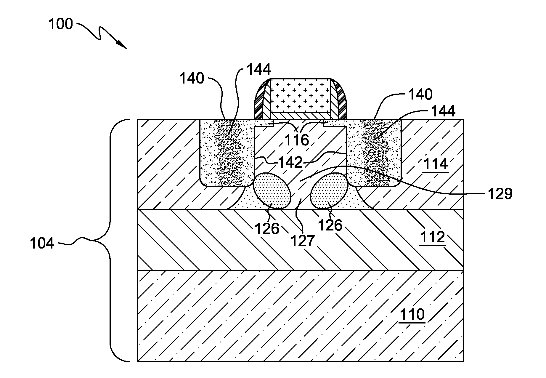
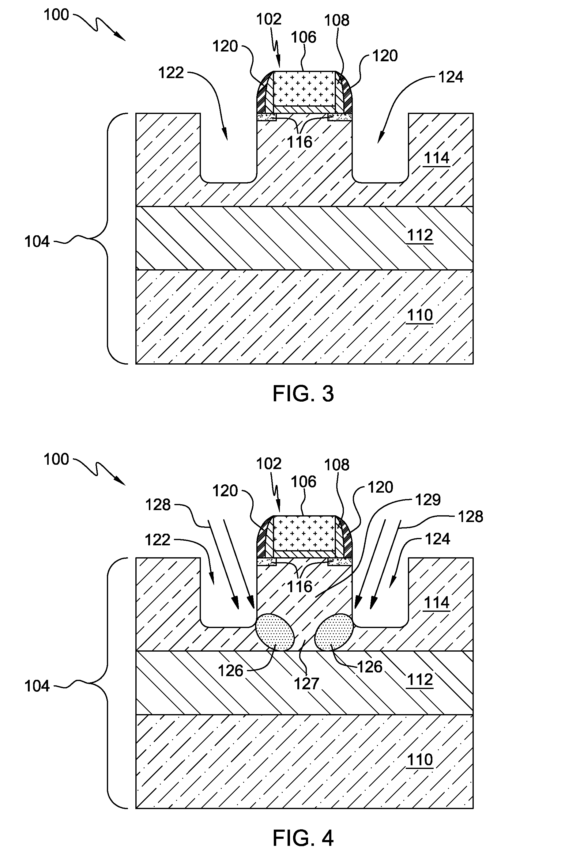
[0003]The various advantages and purposes of the exemplary embodiments as described above and hereafter are achieved by providing, according to a first aspect of the exemplary embodiments, a method of forming a field effect transistor (FET) structure. The method includes forming recesses for a source and a drain of a gate structure on a semiconductor substrate, the FET structure having a body underneath the gate structure and between the source and drain recesses; halo implanting regions through the source and drain recesses and into the bottom of the source and drain recesses, the halo implanted regions being underneath the gate stack and located at a bottom of the FET structure body; implanting junction butting at the bottom of the source and drain recesses; and filling the source and drain recesses with a doped epitaxial material.
[0004]According to a second aspect of the exemplary embodiments, there is provided a method of forming a field effect transistor (FET) structure. The method includes forming recesses for a source and a drain of a gate structure on a semiconductor substrate, the FET structure having a body portion underneath the gate structure and between the source and drain recesses, wherein the semiconductor substrate is a semiconductor on insulator substrate including a semiconductor layer on a buried oxide layer; halo implanting regions through the source and drain recesses and into the bottom of the source and drain recesses, the halo implanted regions being underneath the gate stack, being at a bottom of the FET body portion and be

Problems solved by technology

In present day semiconductor technology and beyond, high peak junction field, back channel leakage, and under junction leakage are impacting semiconductor reliability.
This is also true for analog devices which need low body resistance but the low body resistance may interfere with threshold voltage.

Method used


Image

  • Fet structures with trench implantation to improve back channel leakage and body resistance
  • Fet structures with trench implantation to improve back channel leakage and body resistance
  • Fet structures with trench implantation to improve back channel leakage and body resistance

Examples


Embodiment Construction

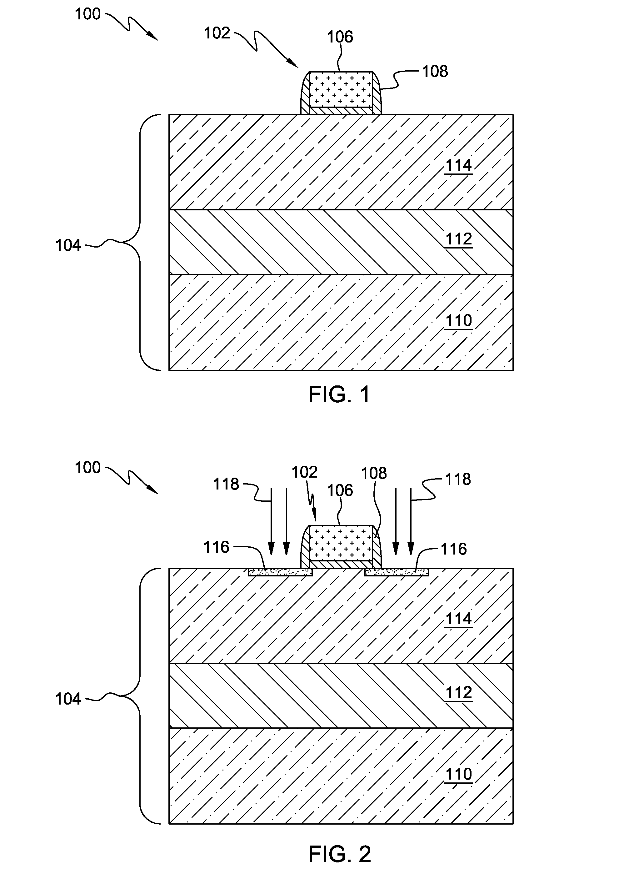
[0017]Referring to the Figures in more detail, and particularly referring to FIG. 1, there is shown a semiconductor structure 100 (an FET in the exemplary embodiment) having a gate structure 102 formed on a semiconductor substrate 104. In an exemplary embodiment, semiconductor substrate 104 is a bulk semiconductor. In a preferred exemplary embodiment, semiconductor substrate 104 is a semiconductor on insulator (SOI) substrate which includes a semiconductor layer 114 on a buried oxide (BOX) layer. The SOI structure is typically built on a semiconductor wafer 110.

[0018]The semiconductor material that makes up semiconductor substrate 104 if it is a bulk semiconductor may include but not be limited to group IV semiconductors such as silicon, silicon germanium or germanium, a III-V compound semiconductor, or a II-VI compound semiconductor. Similarly, in the preferred exemplary embodiment, semiconductor layer 114 and semiconductor wafer 110 may include but not be limited to group IV semic...


PUM


Abstract

An FET structure on a semiconductor substrate which includes forming recesses for a source and a drain of the gate structure on a semiconductor substrate, halo implanting regions through the bottom of the source and drain recesses, the halo implanted regions being underneath the gate stack, implanting junction butting at the bottom of the source and drain recesses, and filling the source and drain recesses with a doped epitaxial material. In exemplary embodiments, the semiconductor substrate is a semiconductor on insulator substrate including a semiconductor layer on a buried oxide layer. In exemplary embodiments, the junction butting and halo implanted regions are in contact with the buried oxide layer. In other exemplary embodiments, there is no junction butting. In exemplary embodiments, halo implants implanted to a lower part of the FET body underneath the gate structure provide higher doping level in lower part of the FET body to reduce body resistance, without interfering with FET threshold voltage.

Description

BACKGROUND[0001]The present invention relates to the field of improving the parasitic leakage of MOSFET (metal oxide semiconductor field effect transistor) structures for semiconductors and, more particularly, relates to FET (field effect transistor) structures and processes having features to reduce leakage in the back channel of the FET, to reduce leakage under the source / drain junction and to reduce FET body resistance without interfering with the threshold voltage of the FET structure.[0002]In present day semiconductor technology and beyond, high peak junction field, back channel leakage, and under junction leakage are impacting semiconductor reliability. This is particularly true for eDRAM which need back gating or side gating well controlled for high retention and yield and SRAM semiconductor structures. This is also true for analog devices which need low body resistance but the low body resistance may interfere with threshold voltage.BRIEF SUMMARY[0003]The various advantages ...

Claims


Application Information

Patent Timeline
IPC IPC(8): H01L29/06H01L21/336
CPCH01L21/26586H01L27/1203H01L29/0847H01L29/7833H01L29/165H01L29/66636H01L29/1083
Inventor FRIED, DAVID MJOHNSON, JEFFREY B.MCSTAY, KEVINPARRIES, PAUL C.PEI, CHENGWENWANG, GANWANG, GENGZHANG, YANLI
Owner IBM CORP
Learn More