Heat-radiating substrate and method for manufacturing the same
a technology of heat-radiating substrate and manufacturing method, which is applied in the direction of printed circuit manufacturing, semiconductor/solid-state device details, conductive pattern formation, etc., can solve the problems of limited use of base plate raw materials, inability to form alumina layers on copper plates, and inability to use aluminum or aluminum alloys. achieve the effect of improving heat-radiation characteristics and high thermal conductivity
- Summary
- Abstract
- Description
- Claims
- Application Information
AI Technical Summary
Benefits of technology
Problems solved by technology
Method used
Image
Examples
first embodiment
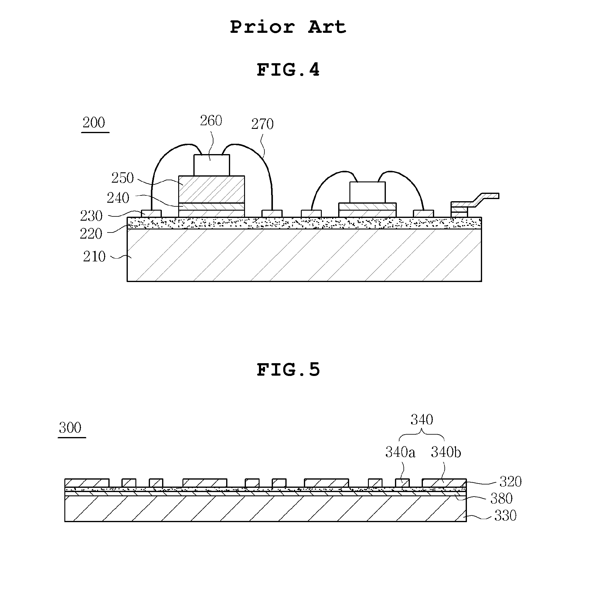
[0048]FIG. 5 is a sectional view showing a heat-radiating substrate according to the present invention.
[0049]As shown in FIG. 5, the heat-radiating substrate 300 according to this embodiment includes a copper substrate 330, an alumina layer 320 formed on one side of the copper substrate 330, and a first circuit layer 340 formed on the alumina layer 320. Here, the first circuit layer 340 includes a first circuit pattern 340a and a first pad 340b. Further, the heat-radiating substrate 300 may further include a seed layer 380 formed between the copper substrate 330 and the alumina layer 320.
[0050]The copper substrate 330, which is a base member of the heat-radiating substrate 300, serves to discharge the heat emitted from a heat-generating element to the atmosphere. Since the copper substrate 330 has high strength compared to a resin substrate, it is highly resistant to the stress externally applied to the heat-radiating substrate 300. Further, in terms of thermal conductivity, aluminu...
second embodiment
[0056]FIG. 6 is a sectional view showing a heat-radiating substrate according to the present invention.
[0057]As shown in FIG. 6, the heat-radiating substrate 400 according to this embodiment includes a copper substrate 330, an alumina layer 320 formed on one side of the copper substrate 330, a first circuit layer 340 formed on the alumina layer 320, and a second circuit layer 350 formed on the first circuit layer 340. Here, the first circuit layer 340 includes a first circuit pattern 340a and a first pad 340b, and the second circuit layer 350 includes a second circuit pattern 350a corresponding to the first circuit pattern 340a and a second pad 350b corresponding to the first pad 340b. Further, the heat-radiating substrate 400 may further include a seed layer 380 formed between the copper substrate 330 and the alumina layer 320.
[0058]Descriptions of the copper substrate 330, the alumina layer 320 and the seed layer 380 in the heat-radiating substrate 400 according to this embodiment...
PUM
| Property | Measurement | Unit |
|---|---|---|
| heat- | aaaaa | aaaaa |
| heat-radiating | aaaaa | aaaaa |
| thermal conductivity | aaaaa | aaaaa |
Abstract
Description
Claims
Application Information
 - R&D
- Intellectual Property
- Life Sciences
- Materials
- Tech Scout
- Unparalleled Data Quality
- Higher Quality Content
- 60% Fewer Hallucinations
Browse by: Latest US Patents, China's latest patents, Technical Efficacy Thesaurus, Application Domain, Technology Topic, Popular Technical Reports.
© 2025 PatSnap. All rights reserved.Legal|Privacy policy|Modern Slavery Act Transparency Statement|Sitemap|About US| Contact US: help@patsnap.com


