
Through-silicon via testing structure

Active Publication Date: 2012-01-19
GLOBAL UNICHIP CORPORATION +1
View PDF1 Cites 7 Cited by
  • Summary
  • Abstract
  • Description
  • Claims
  • Application Information

AI Technical Summary

Benefits of technology

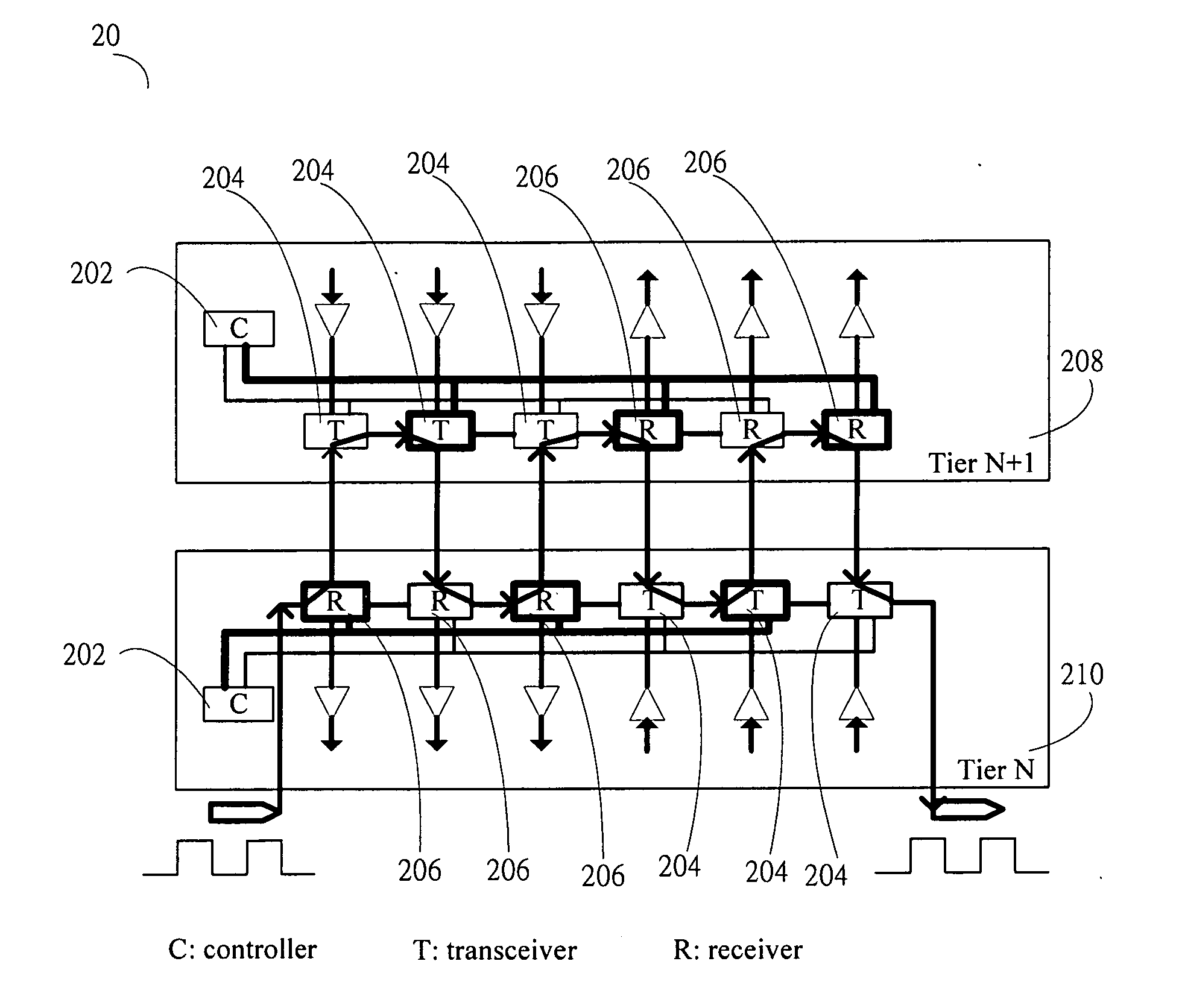
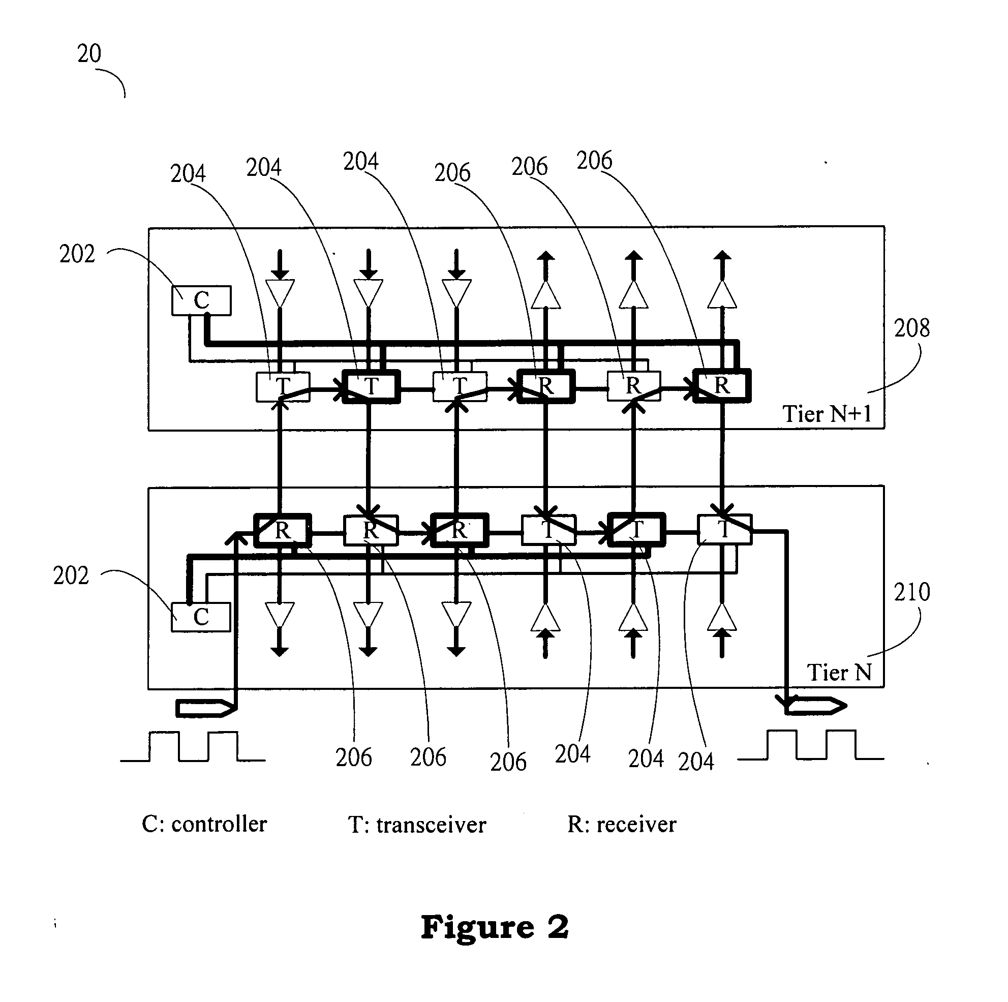
[0007]The purpose of this invention is to provide a through-silicon via (TSV) testing structure. According to the testing structure, it is able to simplify the test procedure and used elements.
[0008]Another purpose of this invention is to provide a through-silicon via testing structure for simplifying its testing structure without requiring many complicated control instructions.

Problems solved by technology

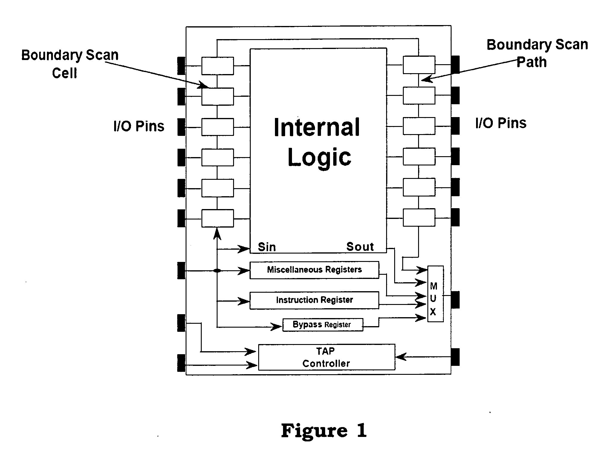
However, the conventional Boundary-Scan test is very complicated, which needs several sequential and combination circuits, thus it needs more space for the test.
The test timing is not efficient as well.

Method used


Image

  • Through-silicon via testing structure
  • Through-silicon via testing structure
  • Through-silicon via testing structure

Examples


Embodiment Construction

[0021]Some embodiments of the invention will be described as follows in detail. However, except the following description, the invention can also be implemented in other embodiments widely. Furthermore, the scope of the invention is not limited by the embodiments. The latter scope of patent will be used as the basis. Moreover, in order to provide clearer description and more intelligible invention, the diagrams in Figures are not drawn in accordance with the relative size. Some sizes and other relevant scales have already been overstated. The unrelated detail parts are also not drawn totally, in order to simplify the diagrams.

[0022]FIG. 2 shows the main element circuit diagram for the through-silicon via testing structure of the invention. The through-silicon via testing structure 20 includes a plurality of controllers 202, a plurality of transmitters 204 and a plurality of receivers 206 mainly. The first connection direction control module 208 and the second connection direction co...


PUM


Abstract

A through-silicon via (TSV) testing structure is disclosed herein and includes a plurality of controllers, a plurality of transmitters and a plurality of receivers. The controllers are configured to output a first controlling signal and a second controlling signal. The transmitters are respectively connected to the output end of the through-silicon via and one of the controllers, and output a testing output signal in accordance with the first controlling signal and the second controlling signal. The receivers are respectively connected to the input end of the through-silicon via and another one of the controllers, and input a testing input signal in accordance with the first controlling signal and the second controlling signal.

Description

BACKGROUND OF THE INVENTION[0001]1. Field of the Invention[0002]This invention relates to a through-silicon via (TSV) testing structure, particularly to a through-silicon via (TSV) testing structure with simplifying test procedure.[0003]2. Description of the Prior Art[0004]The system in package (SIP) is one of main packaging techniques at present, because the SIP is able to use more advanced off-line mounted way (such as through-silicon via (TSV) etc.) in semiconductor process. Due to the process miniaturization and limitation of dielectric material, the heap packaging technology of the three-dimensional (3D) stack packaging has already been considered as the key point for making high efficient chip with smaller size. The through-silicon via uses wafer stacking through vertical conduction, in order to reach the electric interconnection among the chips. The through-silicon via can provide shorter route and lower resistance and inductance than line connection, which is more suitable f...

Claims


Application Information

Patent Timeline
IPC IPC(8): H01L23/48
CPCG01R31/318505
Inventor CHANG, MING-TUNGTSAI, MIN-HSIUTSENG, CHIH-MOU
Owner GLOBAL UNICHIP CORPORATION
Learn More