Narrow-band tunable radio frequency (RF) power amplifiers and related methods
a radio frequency and narrow band filter technology, applied in amplifiers, amplifiers with semiconductor devices/discharge tubes, electrical devices, etc., can solve problems such as the need for a narrow band filter, the loss of signal gain and noise in certain frequency bands, and the increase of the cost and size requirements of communication devices configured to operate in multiple frequency bands
- Summary
- Abstract
- Description
- Claims
- Application Information
AI Technical Summary
Benefits of technology
Problems solved by technology
Method used
Image
Examples
embodiment 350
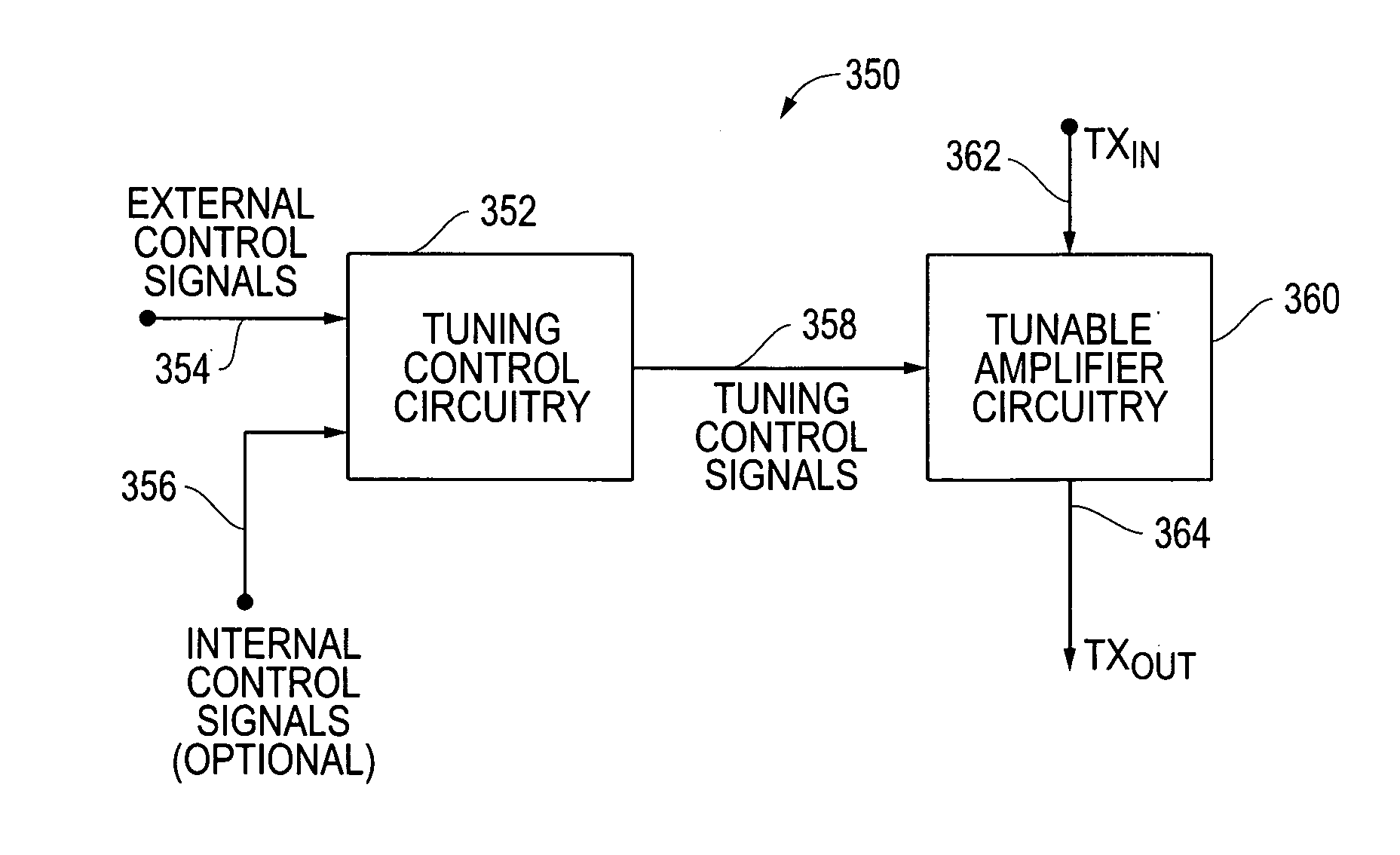
[0044]FIG. 3E is a block diagram of an embodiment 350 for control circuitry configured to provide tuning control signals. As depicted, tunable amplifier circuitry 360 for the PA receive an input transmit signal (TXIN) 362 and produce an amplified transmit output signal (TXOUT) 364. The tunable amplifier circuitry 360 also receive tuning control signals 358 that are used to tune the gain response for the tunable amplifier circuitry 360. The tuning control signals are provided by tuning control circuitry 352. The tuning control circuitry 352 can be controlled using external control signals 354 that can be provided through an external interface. The external interface can be any desired interface for providing band control signals to the PA. The tuning control circuitry 352 can also be controlled in part through one or more internal control signals 356, if desired. Further variations could also be provided while still utilizing the narrow band tunable PA techniques described herein.
[00...
embodiment 400
[0046]FIG. 4A is a circuit diagram of an embodiment 400 for a variable capacitor implementation for lower voltage signals. As depicted, the variable capacitor includes a plurality of capacitors (C0, C1, C2 . . . CN) that are coupled in parallel between a signal line 402 and a signal line 404, such as ground. These capacitors (C0, C1, C2 . . . CN) can be selectably included or excluded from the overall variable capacitance 406 through transistor switches that are controlled by digital control signals (D0, D1, D2 . . . DN). In particular, a capacitor C0 is coupled to signal line 402 and to ground 404 through a transistor switch that is controlled by signal D0. A capacitor C1 is coupled between a signal line 402 and ground 404 through a transistor switch that is controlled by signal D1. A capacitor C2 is coupled between a signal line 402 and ground 404 through a transistor switch that is controlled by signal D2. This continues until finally a capacitor CN is coupled between a signal li...
embodiment 500
[0048]FIG. 5 provides a flow diagram of an embodiment 500 for a process flow for adjusting the gain response for a narrow band tunable PA as described herein. In block 502, a desired frequency band of operation is selected for the communication device and the narrow band tunable PA. In block 504, tuning control signals are provided for the tunable PA based upon the desired frequency band of operation. In block 506, the gain response of the narrow band tunable PA is adjusted by circuitry within the tunable PA. And in block 508, the narrow band tunable PA is operated in the selected band to amplify transmit signals for the selected frequency band of operation. It is noted that a wide variety of different or additional processes could be implemented while still taking advantage of then narrow band tunable PAs described herein.
PUM
 Abstract
Description
Claims
Application Information
 - R&D
- Intellectual Property
- Life Sciences
- Materials
- Tech Scout
- Unparalleled Data Quality
- Higher Quality Content
- 60% Fewer Hallucinations
Browse by: Latest US Patents, China's latest patents, Technical Efficacy Thesaurus, Application Domain, Technology Topic, Popular Technical Reports.
© 2025 PatSnap. All rights reserved.Legal|Privacy policy|Modern Slavery Act Transparency Statement|Sitemap|About US| Contact US: help@patsnap.com


