
Semiconductor device and method for manufacturing same

a technology of semiconductor devices and upper electrodes, applied in the direction of semiconductor devices, electrical apparatus, transistors, etc., can solve the problems of insufficient research on the electrode materials used for the formation of electrodes and allowing for reduced contact resistance, and the difficulty of obtaining an appropriate upper electrode material using ni based or nisi based materials, etc., to achieve high reliability and low electric resistance

Inactive Publication Date: 2012-01-12
SUMITOMO ELECTRIC IND LTD
View PDF6 Cites 42 Cited by
  • Summary
  • Abstract
  • Description
  • Claims
  • Application Information

AI Technical Summary

Benefits of technology

[0007]As described above, when the electrode material and the material for the internal upper electrode are different types of metals, problems may arise in resistance at an interface where the different types of metal materials are in contact with each other; durability of the contact portion in long-term use; and the like. An object of the present invention is to provide a semiconductor device employing silicon carbide and allowing for high reliability (maintenance of initially low electric resistance or the like) even in long-team use without any problem taking place in a contact portion of different types of metals, i.e., an electrode material and an internal upper electrode material which are different from each other.Means for Solving the Problems

Problems solved by technology

In the case of using SiC, electrode materials used for formation of electrodes and allowing for reduced contact resistance have not been sufficiently found, as compared with a case of using silicon, which has been used commonly and traditionally.
However, in the case of SiC, it is difficult to use Al for both an ohmic electrode and an internal upper electrode because good ohmic contact between SiC and Al is hardly obtained at a temperature not more than the melting point of Al.
Further, the above-described Ni based or NiSi based material is not used for an internal upper electrode because each of them is not so low in electric resistance and it is difficult to obtain an appropriate upper electrode material using the Ni based or NiSi based material.
In addition, the Ni based material is less likely to achieve good ohmic contact with p type SiC.

Method used


Image

  • Semiconductor device and method for manufacturing same
  • Semiconductor device and method for manufacturing same
  • Semiconductor device and method for manufacturing same

Examples


first embodiment

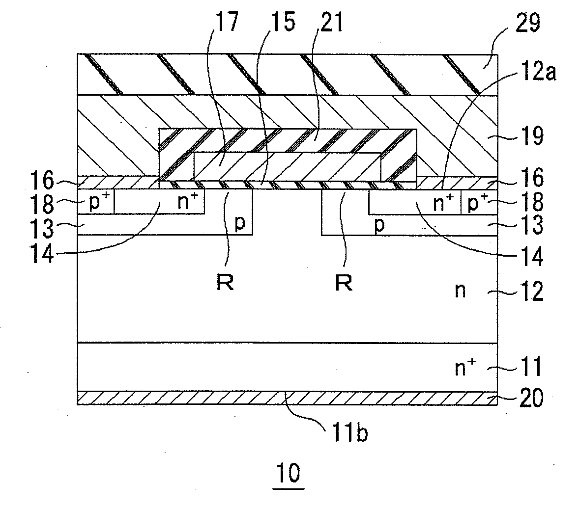
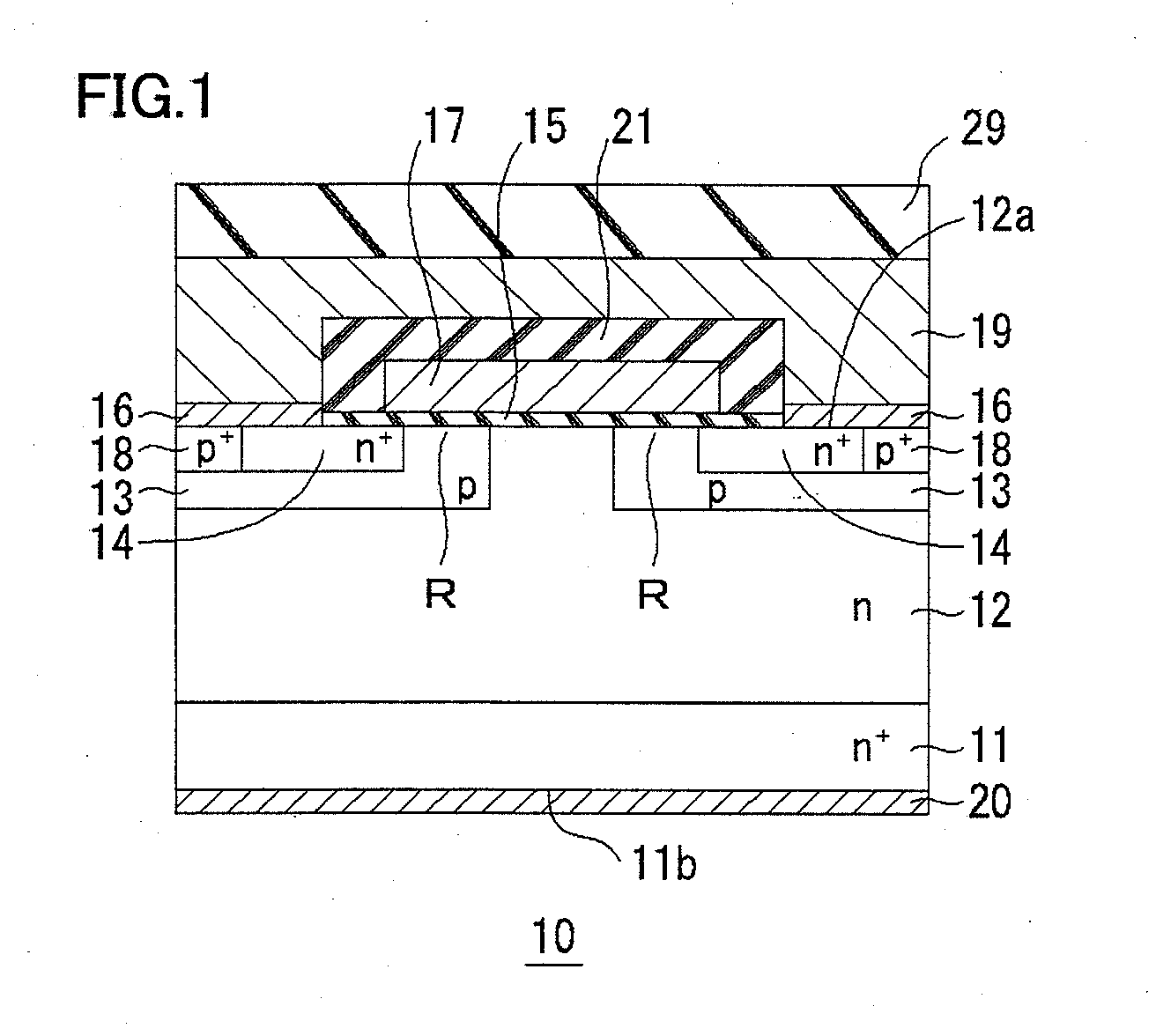
[0039]FIG. 1 is a cross sectional view showing a MOSFET, which is a semiconductor device in a first embodiment of the present invention. In the MOSFET of the present embodiment, silicon carbide (SiC) is used as a semiconductor. The MOSFET includes an n+ type SiC substrate 11, and an n type SiC layer (drift layer) 12 epitaxially grown thereon. N type SiC layer (drift layer) 12 has a thickness of 10 μm, and has an n type impurity concentration of approximately 1×10¹⁶ Cal−3, for example. SiC epitaxial layer 12 has a surface 12a in which p bodies 13, n+SiC source regions 14, p+ SiC regions 18 respectively provided adjacent to source regions 14 are disposed. P bodies 13 are interposed between each of n+ source regions 14 / p+ regions 18 and drift layer region 12.

[0040]A source contact electrode 16 is provided in contact with each of source regions 14 and each of p+ regions 18. An upper source internal electrode 19 is provided in contact with source contact electrode 16. A gate oxide film 1...

second embodiment

[0058]FIG. 9 shows a MOSFET employing SiC, which is a semiconductor device in a second embodiment of the present invention. A difference from the first embodiment lies in that a barrier layer 25 is provided between each of source contact electrodes 16 and upper source internal electrode 19. The other configurations are the same as those of the first embodiment. In the present invention, each of source contact electrodes 16 is formed of TiAlSi alloy, and upper source internal electrode 19 is formed of Al or an Al alloy. Both the metals do not react to each other to generate an intermetallic compound having a high electric resistance. Hence, barrier layer 25 is not much required to block diffusion of elements thereof. Accordingly, barrier layer 25 may be a Ti layer having a thickness of several nm in order to improve adhesion between each of source contact electrodes 16 and upper source internal electrode 19. Further, in order to accommodate to utilization in an environment of high te...

third embodiment

[0064]FIG. 10 is a cross sectional view showing a junction field effect transistor JFET 30, which is a semiconductor device in a third embodiment of the present invention. SiC-JFET 30 has a structure in which the following epitaxial layers are stacked: an n type substrate 31, a first p type layer 32, an n type layer 33, and a second p type layer 34.

[0065]First p type layer 32 may have a thickness of approximately 10 μm and have a p type impurity concentration of approximately 7.5×1015 cm−3, for example. N type layer 33 may have a thickness of approximately 0.45 μm and have an n type impurity concentration of approximately 2×1017 cm−3, for example. Second p type layer 34 may have a thickness of approximately 0.25 μm and have a p type impurity concentration of approximately 2×1017 cm−3.

[0066]Regions 35, 36, 37 are provided which project from a surface 34a of second p type layer 34 into n type layer 33 through the second p type layer. The thickness of n type layer 33 between each botto...


PUM


Abstract

A semiconductor device employing silicon carbide, and the like are provided. In the semiconductor device, even when an electrode material and an upper electrode material are different, a problem does not take place at an interface at which these different types of metals are in contact with each other, thus obtaining high reliability in long-term use.The semiconductor device includes: a contact electrode 16 in contact with silicon carbides 14, 18; and an upper electrode 19 electrically conductive to the contact electrode. The contact electrode 16 is formed of an alloy including titanium, aluminum, and silicon, the upper electrode 19 is formed of aluminum or an aluminum alloy, and the upper electrode achieves the electric conduction to the contact electrode with the upper electrode making contact with the contact electrode.

Description

TECHNICAL FIELD[0001]The present invention relates to a semiconductor device and a method for manufacturing the semiconductor device. More specifically, the present invention relates to a semiconductor device which employs silicon carbide as a semiconductor, is capable of stably maintaining low electric resistance for a long time, and includes an electrode and an upper electrode, as well as a method for manufacturing such a semiconductor device.BACKGROUND ART[0002]In order to achieve high withstand voltage and low loss in a semiconductor device and utilization thereof under a high temperature environment, development of semiconductor devices employing silicon carbide (SiC) has been conducted. In particular, a switching element for a large current is required to achieve high withstand voltage and low loss. Accordingly, development of vertical type switching elements employing silicon carbide, particularly, vertical type MOSFETs (Metal Oxide Semiconductor Field Effect Transistors) or ...

Claims


Application Information

Patent Timeline
IPC IPC(8): H01L29/24H01L21/04
CPCH01L21/0485H01L29/1608H01L29/808H01L29/66068H01L29/7802H01L29/45H01L29/401H01L29/66045H01L29/772H01L21/0455
Inventor WADA, KEIJITAMASO, HIDETOMASUDA, TAKEYOSHIHONAGA, MISAKO
Owner SUMITOMO ELECTRIC IND LTD
Learn More