
Nanoscale metal oxide resistive switching element

a metal oxide resistive switching and metal oxide technology, applied in the field of nonvolatile switching and memory devices, can solve the problems of incompatibility with cmos processing, limited device size, and limited further device size shrinkage, etc., to achieve low current for programming, reduce power consumption in operation, and flexible thermal budget for device fabrication

Active Publication Date: 2012-01-05
RGT UNIV OF MICHIGAN
View PDF5 Cites 67 Cited by
  • Summary
  • Abstract
  • Description
  • Claims
  • Application Information

AI Technical Summary

Benefits of technology

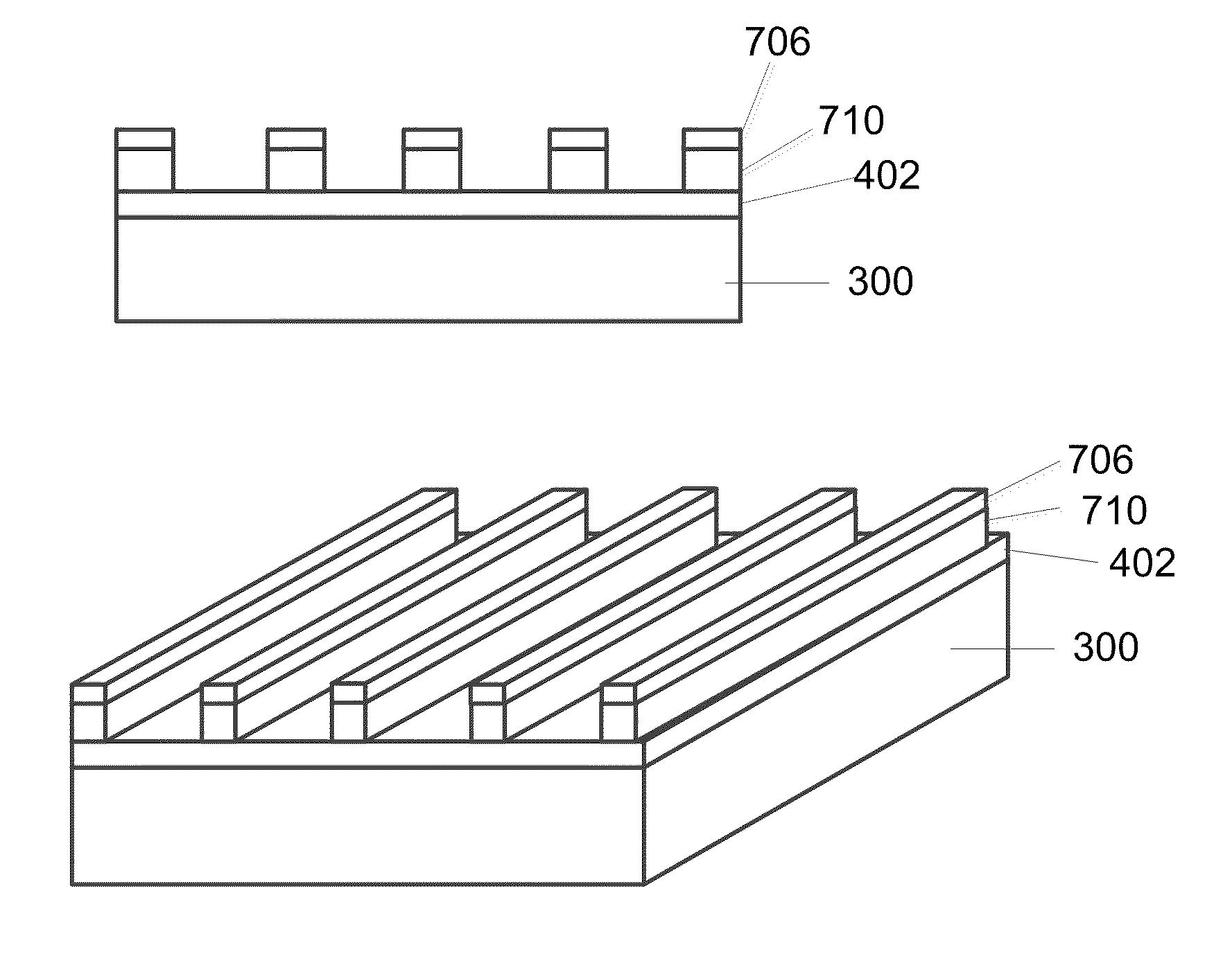
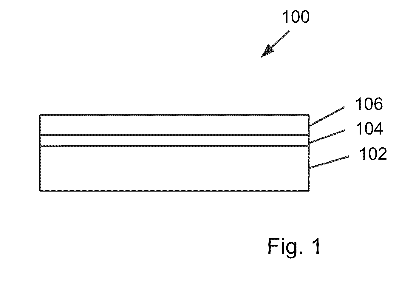
[0006]The present invention is directed to switching and memory devices. More particularly, the present invention in at least some embodiments provides a structure and a method of forming a resistive switching non-volatile memory device using a metal oxide as a switching element. The illustrated embodiment of the present invention has been exemplified using a tungsten oxide material as a switching material. But it should be recognize that other metal oxide materials may also be used and other embodiments of the present invention may have a much broader range of applicability.
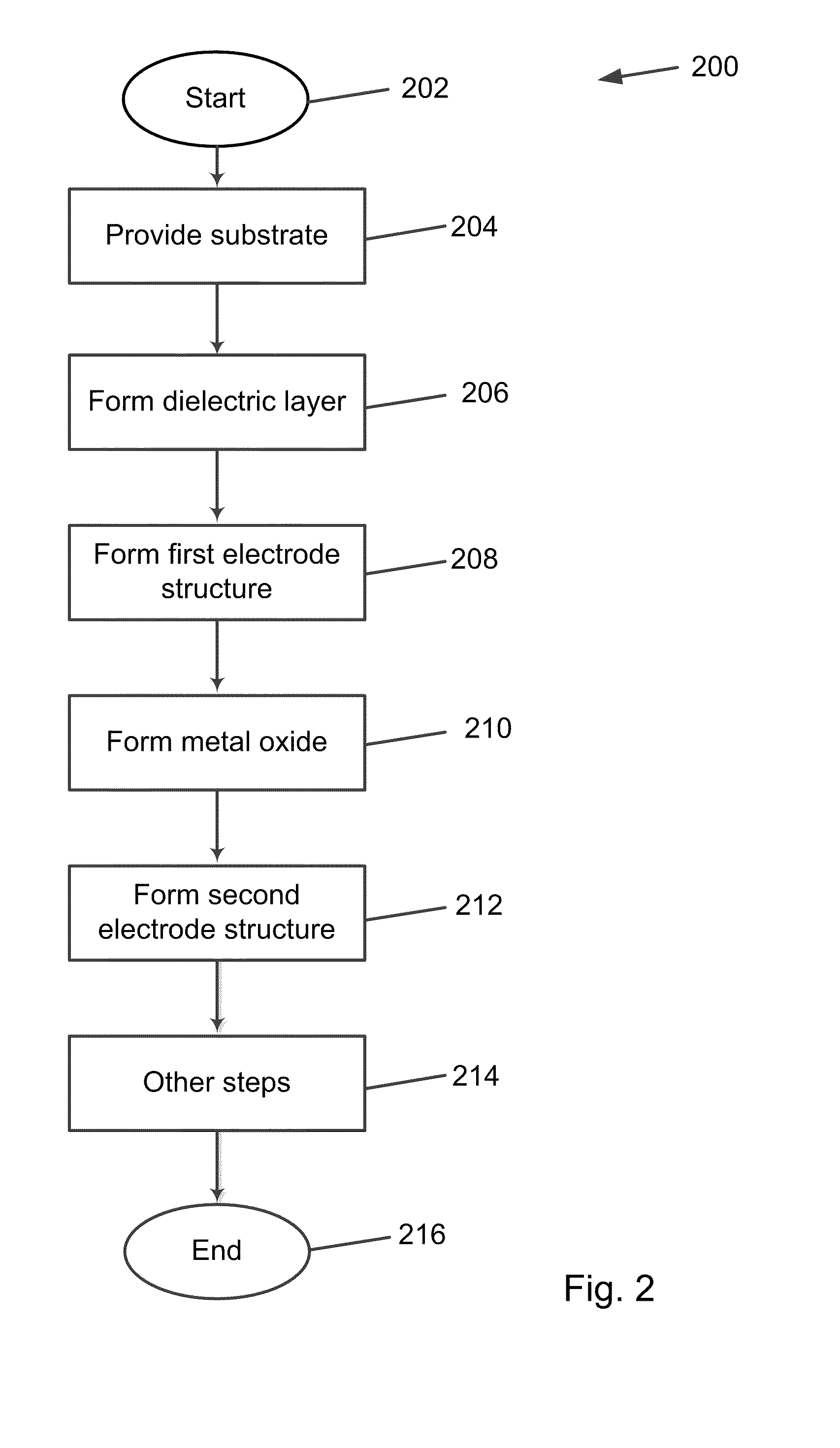
[0009]Many benefits can be achieved by way of the disclosed embodiments of the invention. For example, there is provided a method and a structure to form a switching device, which can be used in a scalable non-volatile memory device in a specific embodiment. Moreover, the present method and device structure can use a low temperature process for electrode formation and provides for a flexible thermal budget for device fabrication. The present device fabrication uses process and materials that are compatible with CMOS processing. Additionally, the present device allows for low current for programming and further reduces power consumption in operation. Additionally, the present device allows for a continuous change in the device resistance (suitable as analog devices) or a sharp change in the device resistance (suitable as digital devices). Depending on the embodiment, one or more benefits may be achieved. One skilled in the art would recognize other variations, modifications, and alternatives.

Problems solved by technology

Recent developments in other memory device structures, such as ferroelectric RAM (Fe RAM), magneto-resistive RAM (MRAM), organic RAM (ORAM), and phase change RAM (PCRAM) are limited by a lack of one or more attributes to high density and high speed memory devices.
For example, Fe-RAM and MRAM are fast switching and having high programming endurance, they are however, not compatible to CMOS processing.
The device size is too large and limited in further device size shrink.
PCRAM uses Joule heating for resistivity switching and therefore incurs an increase in power consumption.
Additionally, PCRAM is also limited by uniformity in phase change control when the device is scaled down.
ORAM suffers from incompatibility with present CMOS processing as well as device reliability and low device yield.

Method used


Image

  • Nanoscale metal oxide resistive switching element
  • Nanoscale metal oxide resistive switching element
  • Nanoscale metal oxide resistive switching element

Examples


Embodiment Construction

[0018]Resistive switching for memory devices usually includes a change of an electric resistance of a switching element sandwiched between two electrodes. The change of the electric resistance of the switching device can be brought about by an injection or redistribution of conductive entities into the switching element when a voltage or a current is applied to the electrodes. Depending on the device structure, the resistance of the switching element may be changed by using mechanisms such as conductor particles formation, electrochemical reactions or cation / anion migration or even oxygen migration in the switching medium, and others, depending on the application.

[0019]Accordingly, the illustrated embodiments are related to switching devices. More particularly, the illustrated embodiments provide a structure and a method for forming a resistive switching device using a metal oxide as a switching material. The switching device has been used in a non-volatile memory device, but other ...


PUM


Abstract

A non-volatile memory device structure. The non-volatile memory device structure comprises a first electrode formed from a first metal material, a resistive switching element overlying the first electrode. The resistive switching element comprises a metal oxide material characterized by one or more oxygen deficient sites. The device includes a second electrode overlying the resistive switching layer, the second electrode being formed from a second metal material. The second electrode is made from a noble metal. The one or more oxygen deficient sites are caused to migrate from one of the first electrode or the second electrode towards the other electrode upon a voltage applied to the first electrode or the second electrode. The device can have a continuous change in resistance upon applying a continuous voltage ramp, suitable for an analog device. Alternatively, the device can have a sharp change in resistance upon applying the continuous voltage ramp, suitable for a digital device.

Description

CROSS-REFERENCE TO RELATED APPLICATIONS[0001]This application claims the benefit of U.S. Provisional Application No. 61 / 358,385, filed Jun. 24, 2010, and U.S. Provisional Application No. 61 / 359,818, filed Jun. 29, 2010. The entire contents of these two applications are hereby incorporated by reference.STATEMENT RELATED TO FEDERAL FUNDING[0002]This invention was made with government support under CCF0621823 awarded by the National Science Foundation. The government has certain rights in the invention.BACKGROUND OF THE INVENTION[0003]The present invention generally relates to non-volatile switching and memory devices. More particularly, the present invention in some embodiments provides a structure and a method of forming resistive switching non-volatile memory devices using a metal oxide as a switching element.[0004]Memory devices are usually transistor based. Current memory devices shrink is primarily driven by a scale down of the transistor. Recent developments in other memory devi...

Claims


Application Information

Patent Timeline
IPC IPC(8): H01L45/00
CPCG11C11/5685G11C13/0007H01L27/2436H01L27/2472H01L45/1675H01L45/1233H01L45/146H01L45/1633H01L45/08H10B63/82H10B63/30H10N70/24H10N70/826H10N70/8833H10N70/028H10N70/063
Inventor LU, WEIJO, SUNG HYUN
Owner RGT UNIV OF MICHIGAN
Learn More