
Display Drivers

a technology of display drivers and drivers, applied in static indicating devices, instruments, optics, etc., can solve the problems of limiting the range of substrates that can be used and relatively low mobility, and achieve the effect of reducing the loss of substrate area

Inactive Publication Date: 2011-12-01
CAMBRIDGE DISPLAY TECH LTD
View PDF17 Cites 4 Cited by
  • Summary
  • Abstract
  • Description
  • Claims
  • Application Information

AI Technical Summary

Benefits of technology

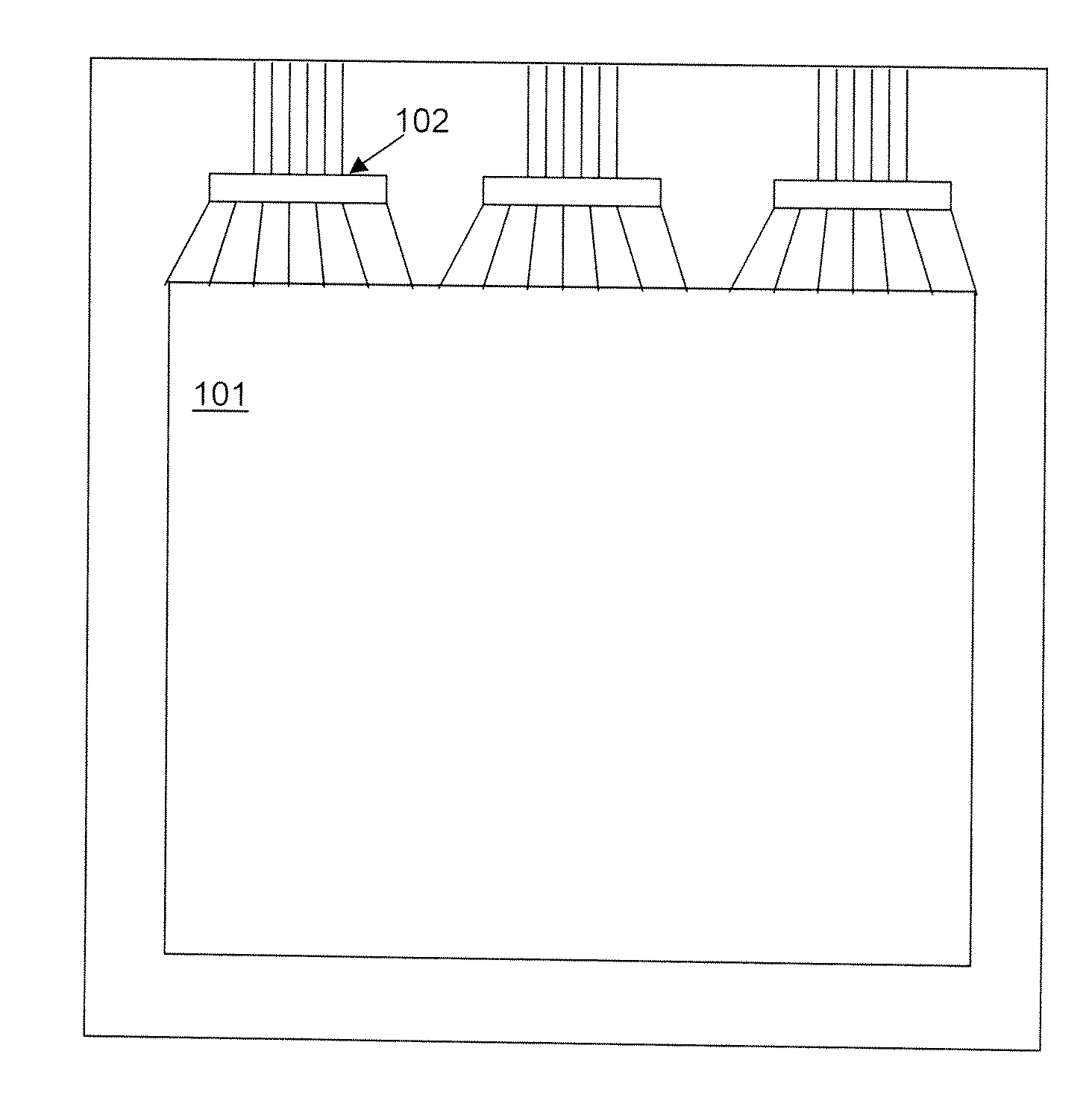
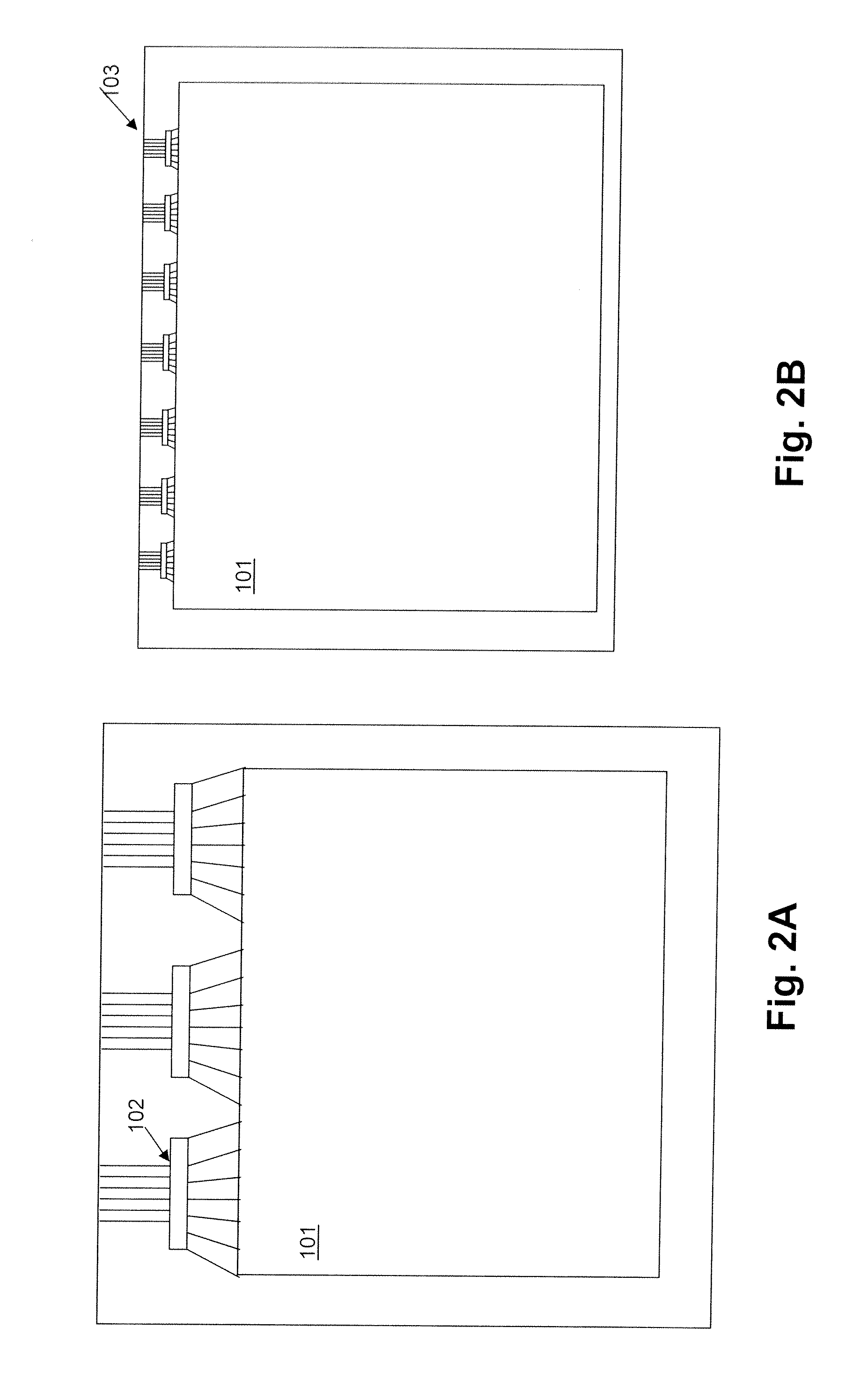
[0017]According to one embodiment, there is a reduction in the substrate area lost to fan-in and fan-out connections through the use of an array of driver chiplets driven by a driver located outside of the active display matrix area.

Problems solved by technology

LIPS has high mobility but can be non-uniform and requires high processing temperatures which limits the range of substrates that it can be used with.
Amorphous silicon does not require such high processing temperatures, however its mobility is relatively low, and can suffer from non-uniformities during use due to aging effects.
Moreover, backplanes formed from either LIPS or a-Si both require processing steps such as photolithography, cleaning and annealing that can damage the underlying substrate.

Method used


Image

  • Display Drivers
  • Display Drivers
  • Display Drivers

Examples


Embodiment Construction

Chiplet Material

[0023]The chiplets may be formed from semiconductor wafer sources, including bulk semiconductor wafers such as single crystalline silicon wafers, polycrystalline silicon wafers, germanium wafers; ultra thin semiconductor wafers such as ultra thin silicon wafers; doped semiconductor wafers such as p-type or n-type doped wafers and wafers with selected spatial distributions of dopants (semiconductor on insulator wafers such as silicon on insulator (e.g. Si—SiO2, SiGe); and semiconductor on substrate wafers such as silicon on substrate wafers and silicon on insulator. In addition, printable semiconductor elements of the present invention may be fabricated from a variety of nonwafer sources, such as a thin films of amorphous, polycrystalline and single crystal semiconductor materials (e.g. polycrystalline silicon, amorphous silicon, polycrystalline GaAs and amorphous GaAs) that is deposited on a sacrificial layer or substrate (e.g. SiN or SiO2) and subsequently annealed,...


PUM

PropertyMeasurementUnit
widthaaaaaaaaaa
widthaaaaaaaaaa
lengthaaaaaaaaaa

Abstract

An active matrix display comprises a display area of the matrix comprising drive circuitry including a control circuit comprising chiplets outside the display area. The output of the control circuit is distributed among the plurality of chiplets. This arrangement is advantageous in that the chiplets allow for a much smaller fan-in and fan-out structure, thus allowing a much larger percentage of the substrate to be devoted to display area.

Description

BACKGROUND[0001]Recent years have seen very substantial growth in the market for displays as the quality of displays improves, their cost falls, and the range of applications for displays increases. This includes both large area displays such as for TVs or computer monitors and smaller displays for portable devices.[0002]The most common classes of display presently on the market are liquid crystal displays and plasma displays although displays based on organic light-emitting diodes (OLEDs) are now increasingly attracting attention due to their many advantages including low power consumption, light weight, wide viewing angle, excellent contrast and potential for flexible displays.[0003]The basic structure of an OLED is a light emissive organic layer, for instance a film of a poly(p-phenylenevinylene) (“PPV”) or polyfluorene, sandwiched between a cathode for injecting negative charge carriers (electrons) and an anode for injecting positive charge carriers (holes) into the organic laye...

Claims


Application Information

Patent Timeline
Patent Type & Authority Applications(United States)
IPC IPC(8): H05B37/02H05K13/00H05K3/30H05B37/00
CPCH01L27/3255Y10T29/49002Y10T29/4913H01L27/3276H10K59/129H10K59/131G02F1/136277G09G3/3225H10K59/12H10K10/46H10K50/30
Inventor BURROUGHES, JEREMYCOATS, STEPHENGREGORY, HAYDNSMITH, EUANCARTER, JULIAN
Owner CAMBRIDGE DISPLAY TECH LTD
Learn More