Strained Semiconductor Device and Method of Making the Same

a technology of semiconductor devices and strainers, applied in the direction of semiconductor devices, electrical devices, transistors, etc., can solve the problem that the effect of mechanical stress on the performance of transistors is not guaranteed for all transistors, and achieve the effect of improving transistor performance and carrier mobilities

Active Publication Date: 2011-11-17
INFINEON TECH AG
View PDF6 Cites 12 Cited by
  • Summary
  • Abstract
  • Description
  • Claims
  • Application Information

AI Technical Summary

Benefits of technology

In the prior art, as described above, trenches are etched next to transistor gates. These trenches are filled with epitaxial SiGe or other material that has a different lattice constant than silicon. Due to the different lattice constants or thermal expansion coefficients, mechanical stress is produced and issued onto the transistor channel, resulting in improved carrier mobilities and thus improved transistor performance.
In one aspect, the present invention provides a self-aligned etching and filling of grooves or recesses in silicon (or another semiconductor) in the neighborhood of a gate. The preferred method assures a uniform length of the trenches resulting in a uniform filling with equivalent amounts of material. One advantage is that the trenches can be designed uniformly over the wafer surface. This allows for good stress optimization.

Problems solved by technology

Therefore, an equal impact of the mechanical stress on the transistor performance is not guaranteed for all transistors.

Method used


Image

  • Strained Semiconductor Device and Method of Making the Same
  • Strained Semiconductor Device and Method of Making the Same
  • Strained Semiconductor Device and Method of Making the Same

Examples


first embodiment

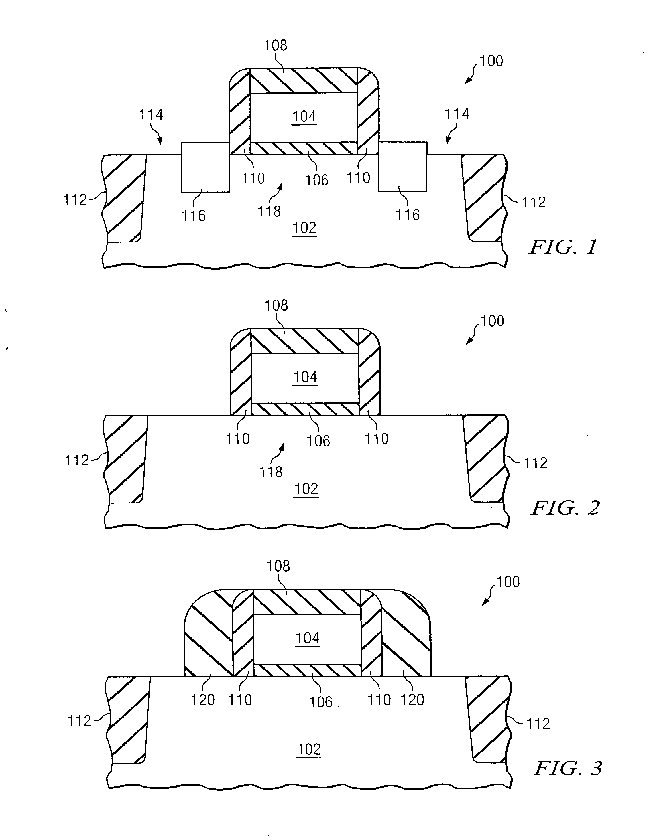
A first embodiment process to fabricate the transistor of FIG. 1 will be described with respect to FIGS. 2-10. This process flow describes preferred manufacturing processes and techniques. As will be recognized by one of skill in the art, a number of variations are possible.

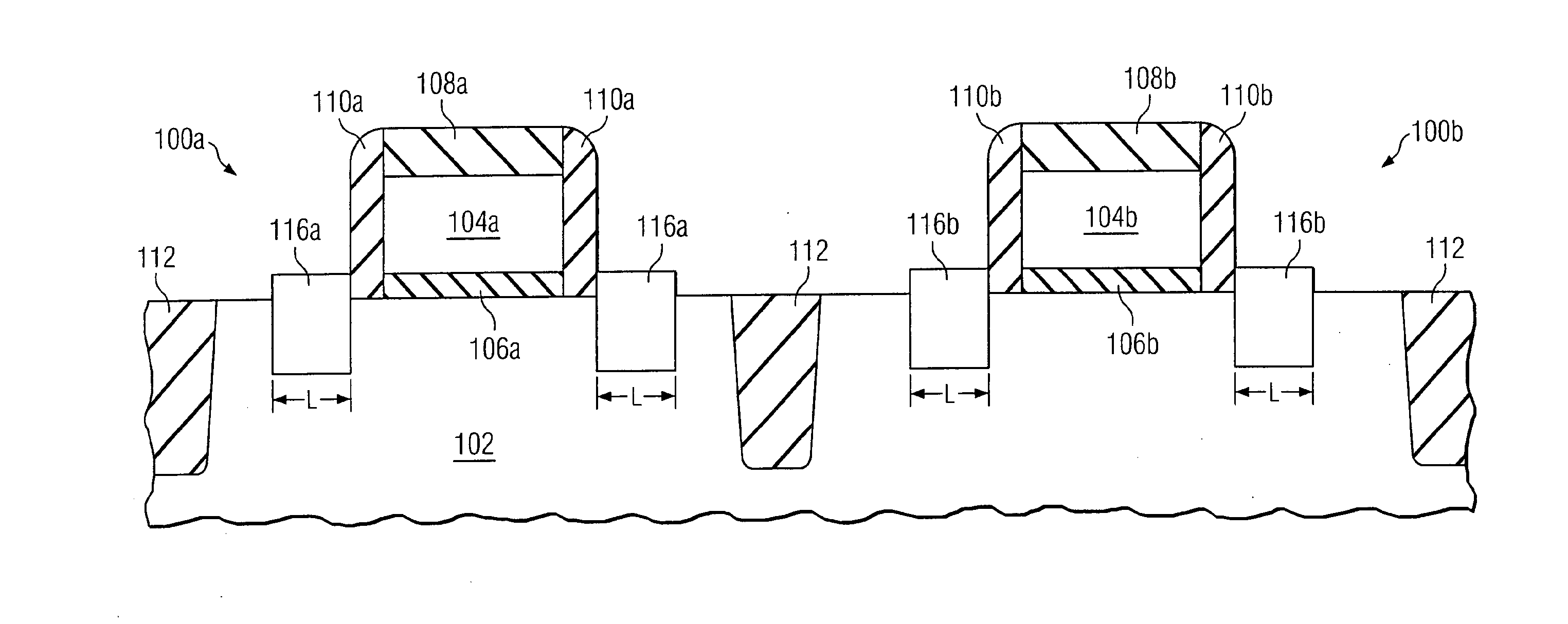
Referring first to FIG. 2, a transistor has been partially fabricated. In particular, STI regions 112 and a gate stack, which includes gate dielectric 106, gate electrode 104, and hard mask layer 108, have been formed using conventional processes. Sidewall spacers 110 have also been formed along sidewalls of the gate electrode 104. These spacers can be formed by conformally depositing an insulating material and anisotropically etching the material. The thickness of the spacer can be determined by the desired dimension of the source / drain extension (or lightly doped source / drain region), which is not explicitly illustrated.

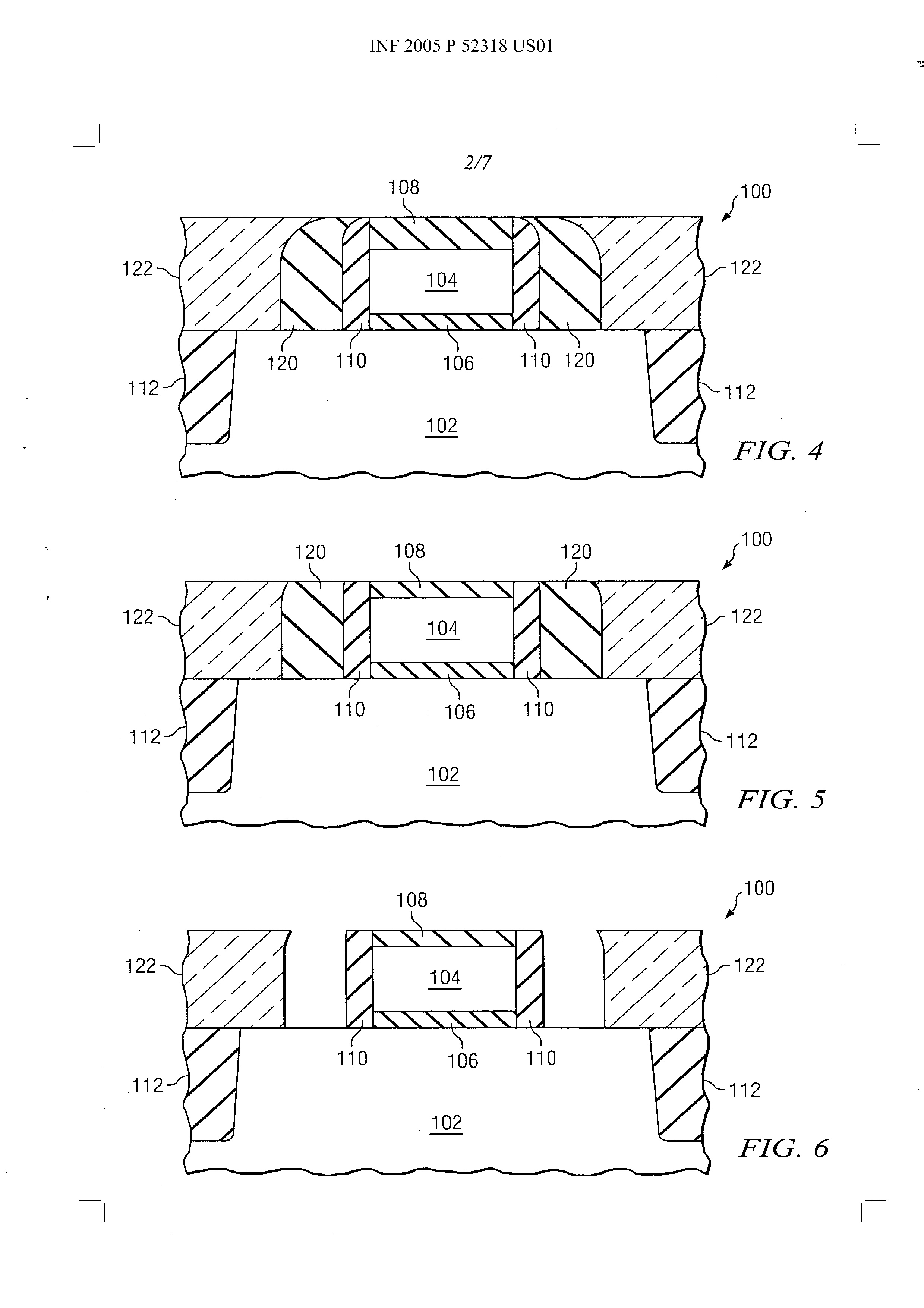
Turning now to FIG. 3, sacrificial sidewall spacers 120 are formed adjacent the sidewall spa...


PUM


Abstract

In a method for forming a semiconductor device, a gate electrode is formed over a semiconductor body (e.g., bulk silicon substrate or SOI layer). The gate electrode is electrically insulated from the semiconductor body. A first sidewall spacer is formed along a sidewall of the gate electrode. A sacrificial sidewall spacer is formed adjacent the first sidewall spacer. The sacrificial sidewall spacer and the first sidewall spacer overlying the semiconductor body. A planarization layer is formed over the semiconductor body such that a portion of the planarization layer is adjacent the sacrificial sidewall spacer. The sacrificial sidewall spacer can then be removed and a recess etched in the semiconductor body. The recess is substantially aligned between the first sidewall spacer and the portion of the planarization layer. A semiconductor material (e.g., SiGe or SiC) can then be formed in the recess.

Description

TECHNICAL FIELDThis invention relates generally semiconductor devices and methods, and more particularly to a strained semiconductor device and a method of making the same.BACKGROUNDSemiconductor devices are used in a large number of electronic devices such as computers, cell phones and others. One of the goals of the semiconductor industry is to continue shrinking the size and increasing the speed of individual devices. Smaller devices can operate at higher speeds since the physical distance between components is smaller. In addition, higher conductivity materials such as copper are replacing lower conductivity materials such as aluminum. One other challenge is to increase the mobility of semiconductor carriers such as electrons and holes.One technique to improve transistor performance is to mechanically strain (i.e., distort) the semiconductor crystal lattice near the charge-carrier channel region. Transistors built on strained silicon, for example, have greater charge-carrier mob...

Claims


Application Information

Patent Timeline
Patent Type & Authority Applications(United States)
IPC IPC(8): H01L27/088H01L21/8234
CPCH01L29/6653H01L29/66636H01L29/7834H01L29/7848H01L29/66477H01L21/823814H01L21/823864H01L27/1203H01L21/823807H01L27/088
Inventor TEWS, HELMUT HORSTSCHENK, ANDRE
Owner INFINEON TECH AG
Why Eureka
Try Eureka