Thin film deposition apparatus, method of manufacturing organic light-emitting display device by using the apparatus, and organic light-emitting display device manufactured by using the method
a thin film and deposition apparatus technology, applied in the direction of discharge tube luminescnet screen, discharge tube/lamp details, vacuum evaporation coating, etc., can solve the problems of difficult to manufacture large organic light-emitting display devices, difficult to achieve high light-emission efficiency with such a structure, and practicably very difficult to form fine patterns in organic thin films. achieve the effect of improving manufacturing yield and deposition efficiency, and easy manufacturing
- Summary
- Abstract
- Description
- Claims
- Application Information
AI Technical Summary
Benefits of technology
Problems solved by technology
Method used
Image

Examples
first embodiment
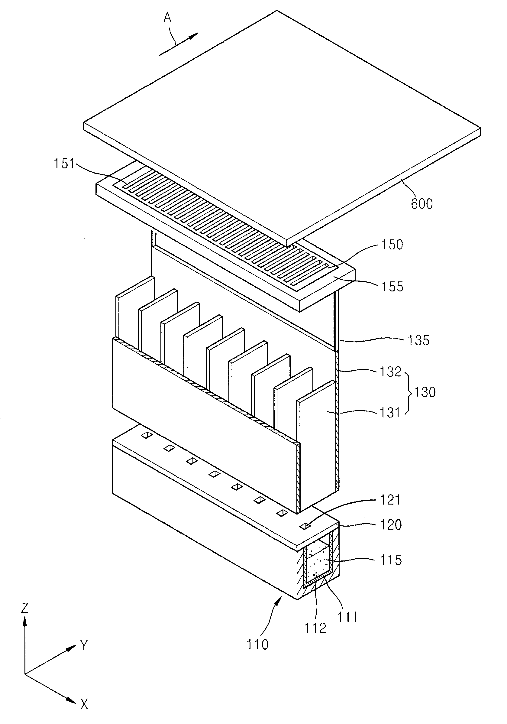
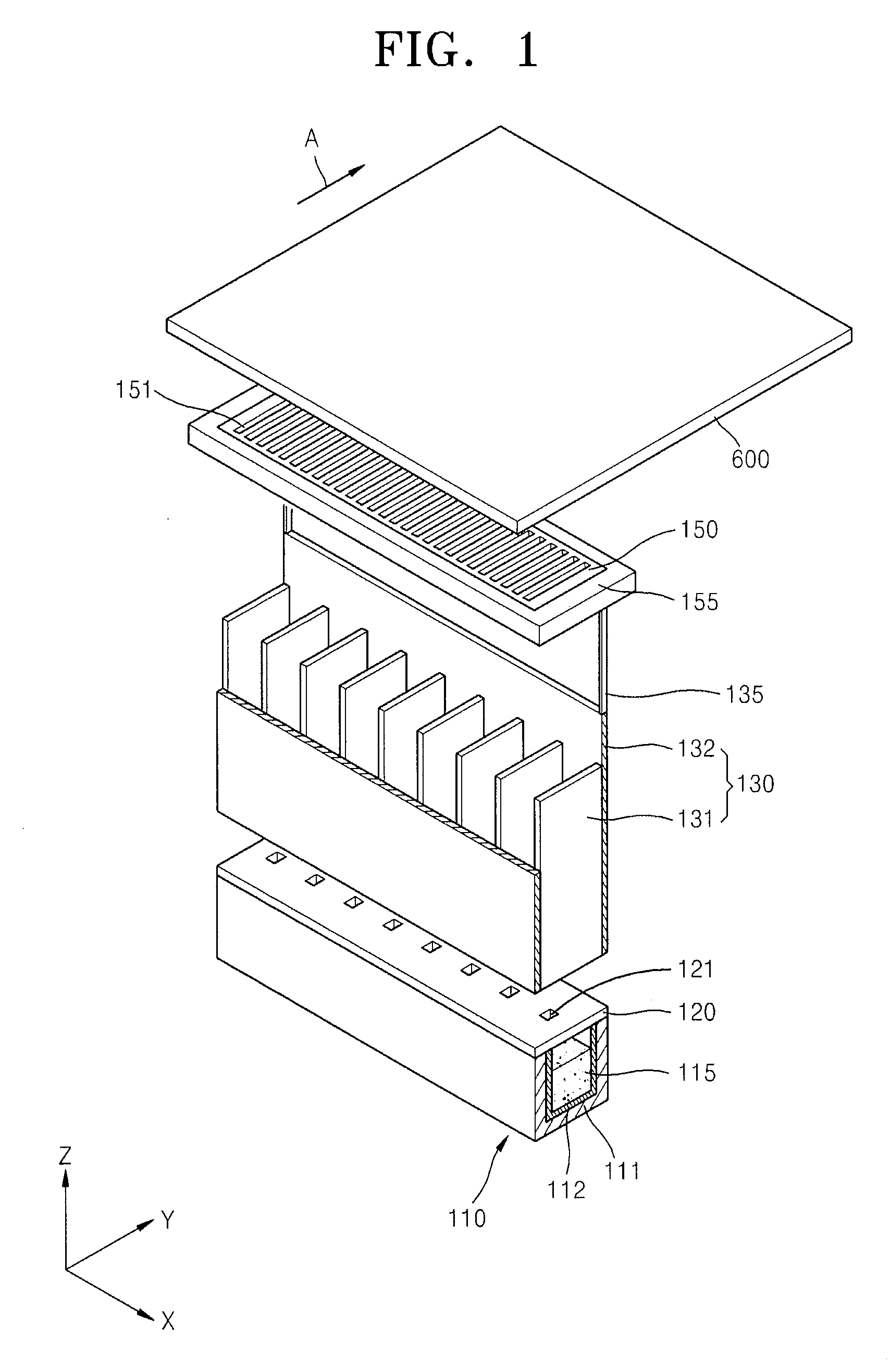
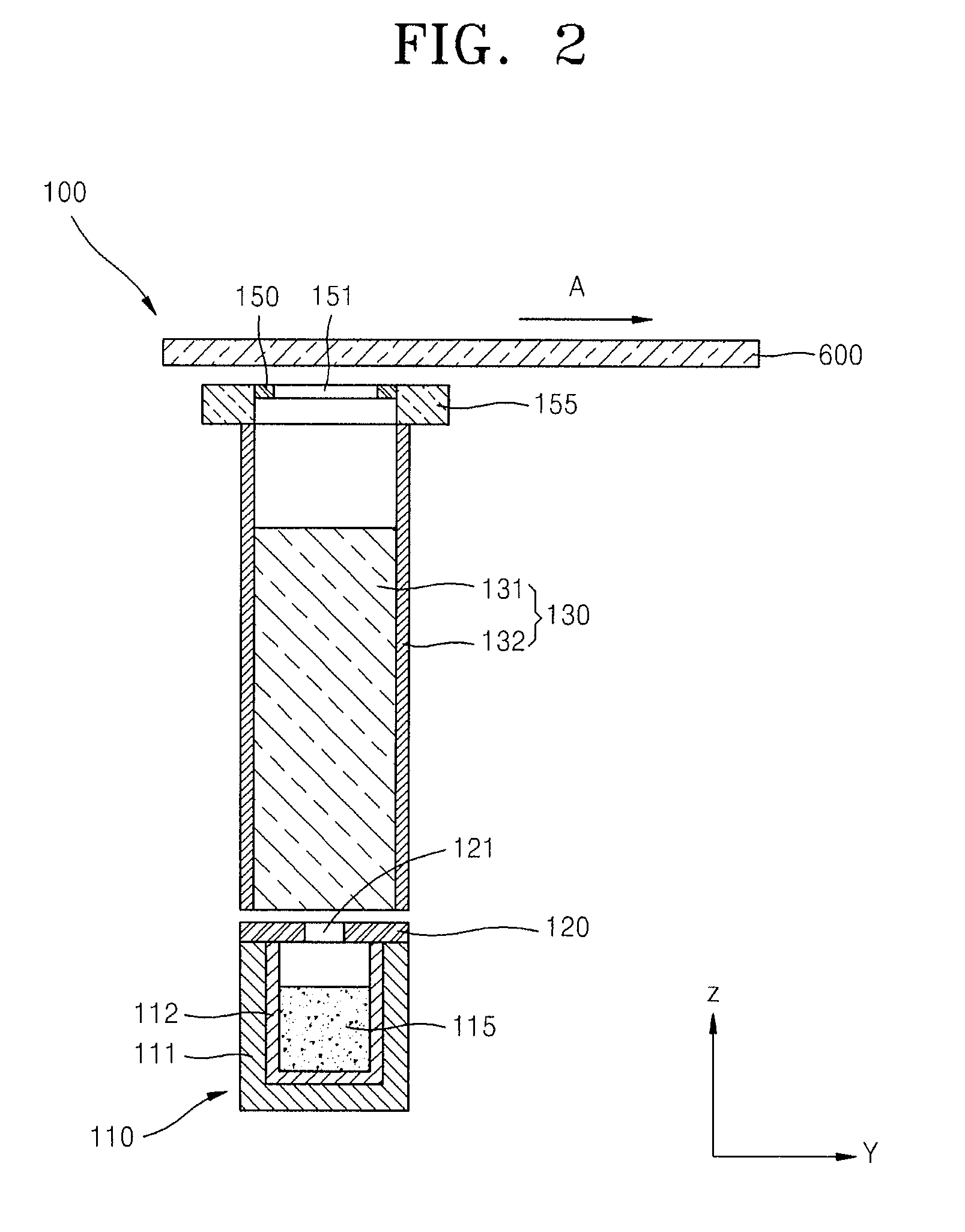
[0038]Turning now to FIGS. 1 through 3, FIG. 1 is a schematic perspective view of a thin film deposition assembly 100 according to the present invention, FIG. 2 is a schematic sectional view of the thin film deposition assembly 100 illustrated in FIG. 1, and FIG. 3 is a schematic plan view of the thin film deposition assembly 100 illustrated in FIG. 1.
[0039]Referring to FIGS. 1, 2 and 3, the thin film deposition assembly 100 according to the first embodiment of the present invention includes a deposition source 110, a deposition source nozzle unit 120, a barrier plate assembly 130, and a patterning slit sheet 150.
[0040]Although a chamber is not illustrated in FIGS. 1, 2 and 3 for the convenience of explanation, all the components of the thin film deposition apparatus 100 may be disposed within a chamber that is maintained at an appropriate degree of vacuum. The chamber is maintained at an appropriate vacuum in order to allow a deposition material to move in a substantially straight ...
second embodiment
[0107]The thin film deposition assembly 700 according to the present invention includes two separate barrier plate assemblies, i.e., the first barrier plate assembly 730 and the second barrier plate assembly 740.
[0108]The plurality of first barrier plates 731 may be arranged parallel to each other at equal intervals in the X-axis direction. In addition, each of the first barrier plates 731 may be formed to extend along a YZ plane in FIG. 10, i.e., perpendicular to the X-axis direction.
[0109]The plurality of second barrier plates 741 may be arranged parallel to each other at equal intervals in the X-axis direction. In addition, each of the second barrier plates 741 may be formed to extend parallel to the YZ plane in FIG. 710, i.e., perpendicular to the X-axis direction.
[0110]The plurality of first barrier plates 731 and second barrier plates 741 arranged as described above partition the space between the deposition source nozzle unit 720 and the patterning slit sheet 750. In the thin...
third embodiment
[0120]As described above, the thin film deposition assembly 1100 according to the present invention performs deposition while being moved relative to the substrate 600. In order to move the thin film deposition assembly 1100 relative to the substrate 600, the patterning slit sheet 1150 must be spaced apart from the substrate 600 (e.g., spaced apart by a predetermined distance).
[0121]As described above, according to the described embodiments of the present invention, a mask is formed to be smaller than a substrate, and deposition is performed while the mask is moved relative to the substrate. Thus, the mask can be easily manufactured. In addition, defects caused due to contact between a substrate and a FMM, which occur in the conventional deposition technique, may be prevented. Furthermore, since it is unnecessary to dispose the FMM in close contact with the substrate during a deposition process, the manufacturing time may be reduced.
[0122]Although not illustrated, a thin film deposi...
PUM
| Property | Measurement | Unit |
|---|---|---|
| temperatures | aaaaa | aaaaa |
| temperature | aaaaa | aaaaa |
| temperature | aaaaa | aaaaa |
Abstract
Description
Claims
Application Information
 - R&D
- Intellectual Property
- Life Sciences
- Materials
- Tech Scout
- Unparalleled Data Quality
- Higher Quality Content
- 60% Fewer Hallucinations
Browse by: Latest US Patents, China's latest patents, Technical Efficacy Thesaurus, Application Domain, Technology Topic, Popular Technical Reports.
© 2025 PatSnap. All rights reserved.Legal|Privacy policy|Modern Slavery Act Transparency Statement|Sitemap|About US| Contact US: help@patsnap.com