
Cutting device for cutting graphene and a method for cutting graphene using a cutting device

Inactive Publication Date: 2011-11-03
HUMBOLDT UNIVET ZU BERLIN
View PDF1 Cites 7 Cited by
  • Summary
  • Abstract
  • Description
  • Claims
  • Application Information

AI Technical Summary

Benefits of technology

[0007]Therefore, a flexible cutting of graphene is enabled, so that predeterminable contours in particular can be realised for cuts in graphene. Thus, it is for example possible to produce an electronic circuit based on graphene.
[0009]A preferred development of the invention provides for the cutting element to be formed with a tip of a probe microscope. This may advantageously be a suitably formed tip, for example a cantilever tip of a scanning force microscope or a tip of a scanning tunneling microscope. It may further be advantageous to provide for the tip to be produced entirely of a catalytically active material. In this manner, a problem of different thermal expansions, which may arise when using materials with different coefficients of thermal expansion, can at least be moderated, for example. This can in particular prevent a problem arising with respect to a contaminating layer on the graphene. By way of example, the tip is produced entirely of tungsten, but other catalytically active materials such as for example metals or alloys thereof can also be provided.
[0014]It is possible to cut graphene in a flexible manner using the cutting device for cutting graphene and method for cutting graphene using a cutting device. In particular, it is possible to predetermine cutting contours and reproducibly implement them. Further, cuts with a roughness of less than 2 nm can be produced. The cutting procedure can be carried out at high speed. The reaction products are harmless or can readily be made harmless. Further, the cutting of graphene using the cutting device and the method is possible relatively inexpensively, as no ultra-high vacuum apparatuses, as are required for example for electron beam lithography, are required.

Problems solved by technology

There is currently no lithographic method for this.
However, it will not be possible in the near future to produce an electronic circuit from a single graphene layer using electron beam lithography.
It is disadvantageous in this method that cutting a nanotube is not possible at a predetermined point, rather cutting takes place randomly.
It is not possible to achieve a predeterminable shaping of graphene using the method described.

Method used


Image

  • Cutting device for cutting graphene and a method for cutting graphene using a cutting device
  • Cutting device for cutting graphene and a method for cutting graphene using a cutting device
  • Cutting device for cutting graphene and a method for cutting graphene using a cutting device

Examples


Embodiment Construction

[0015]The invention is explained in more detail in the following on the basis of preferred exemplary embodiments with reference to figures of a drawing. In the figures:

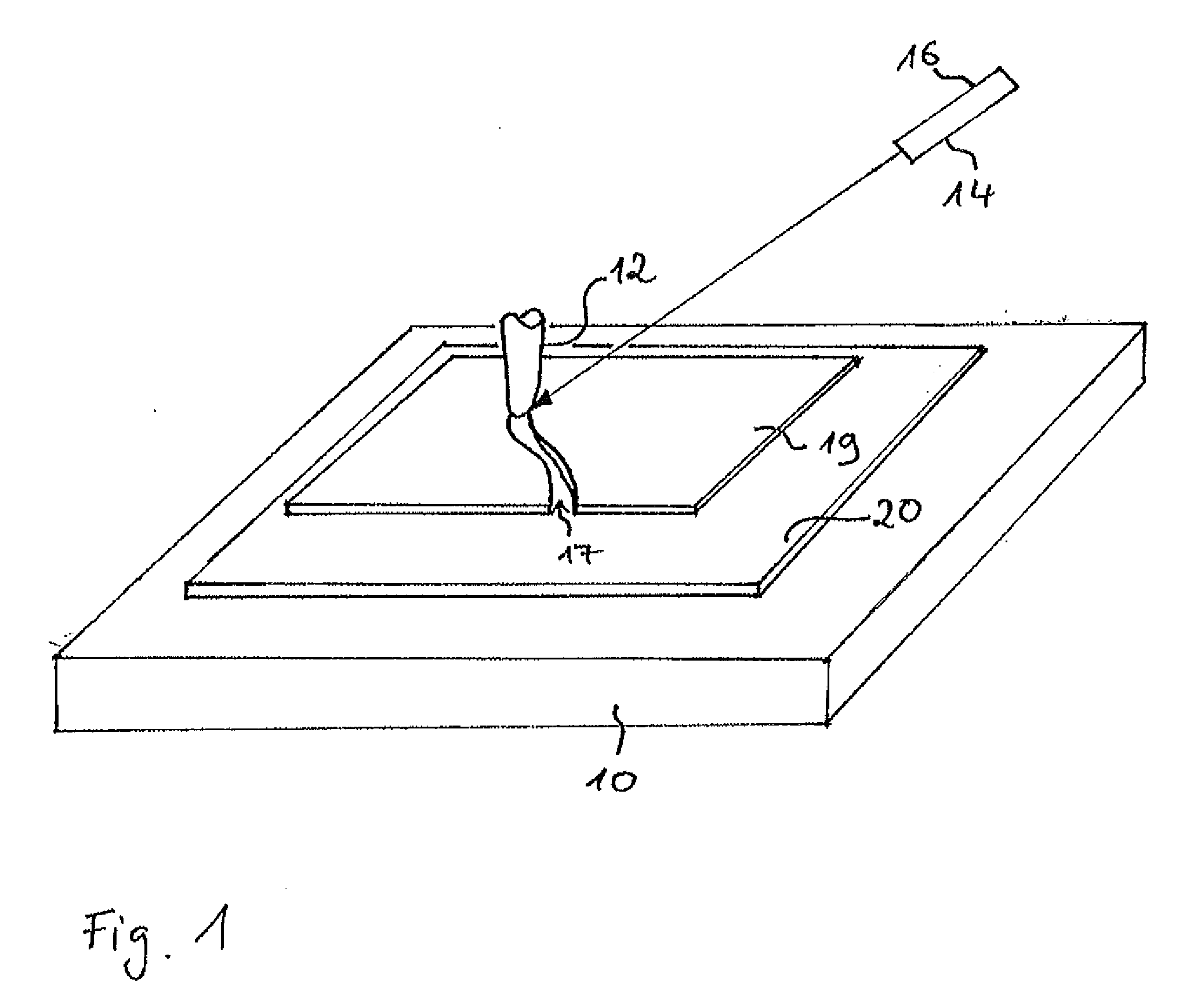
[0016]FIG. 1 shows a cutting device for cutting graphene in a schematic illustration,

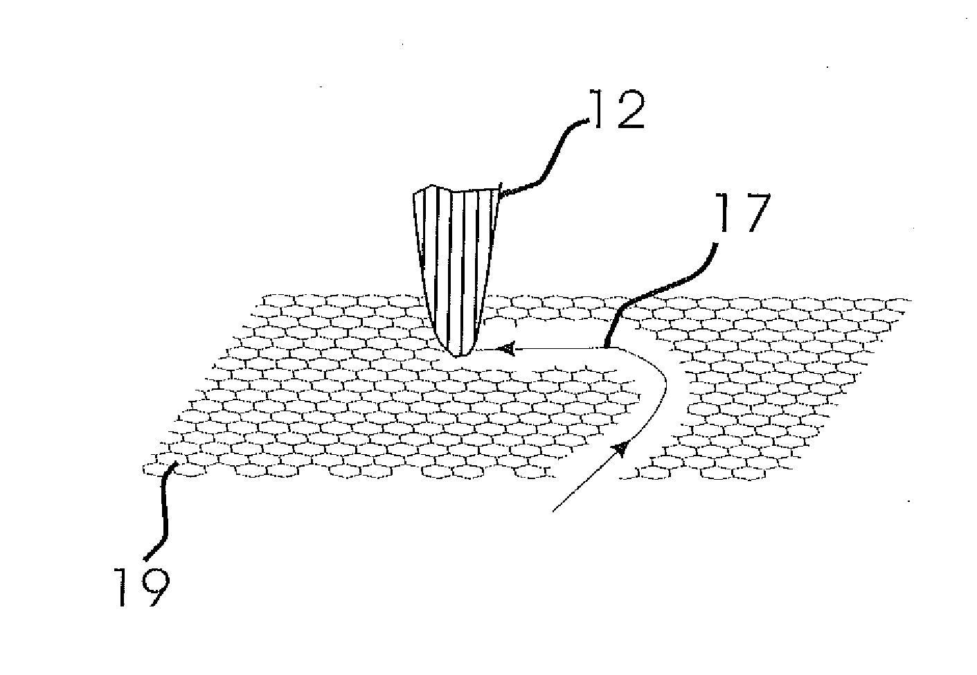
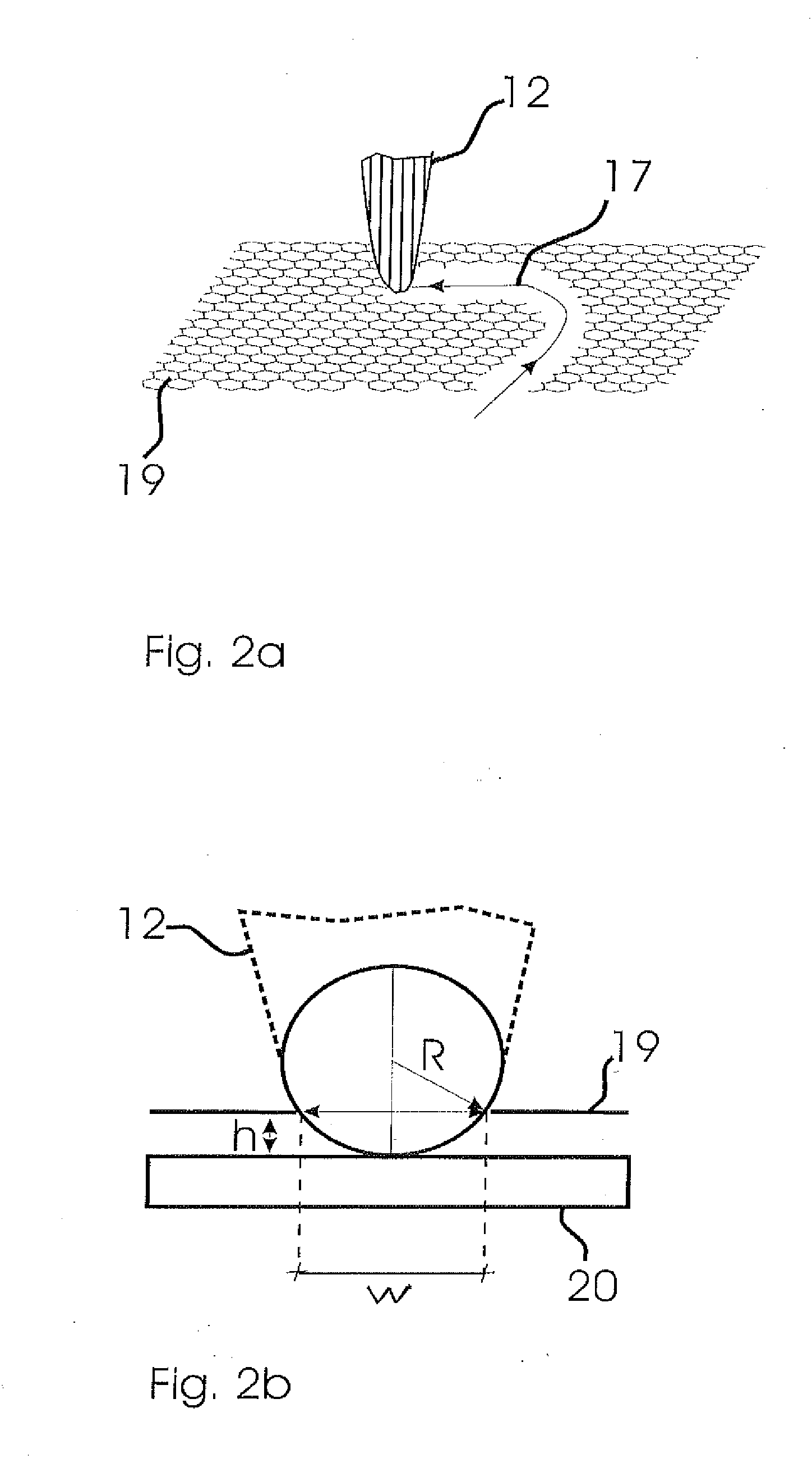
[0017]FIG. 2a shows a further schematic illustration of a cutting procedure with a cutting element of the cutting device,

[0018]FIG. 2b shows a schematic illustration for explaining the connection between a graphene thickness, a radius of curvature of the cutting element at its cutting tip and the width of a cut achieved, and

[0019]FIGS. 3a-g show experimental results and a further schematic illustration of a cutting procedure in an embodiment.

[0020]FIG. 1 shows a cutting device for cutting graphene. A receptacle 10 is configured to accommodate the graphene 19 for cutting. The graphene 19 is for example arranged on an insulating substrate 20. A cutting element 12 is loaded with a catalytically active material, at least in the region of ...


PUM


Abstract

The invention relates to a cutting device for cutting graphene, with a receptacle (10) which is configured to accommodate the graphene (19) for cutting, a cutting element (12) which is loaded with a catalytically active material, at least in the region of a cutting tip, a shifting apparatus, which is configured for shifting the receptacle (10) and the cutting element (12) with the cutting tip relatively to one another, and a heating device (14), which is configured to supply thermal energy during the cutting of the graphene (19) for a catalytic reaction of the graphene in the region of a cutting path with the participation of the catalytically active material.

Description

[0001]The invention relates to a cutting device for cutting graphene and a method for cutting graphene using a cutting device.BACKGROUND OF THE INVENTION[0002]Graphene is a material which consists of thin single-atom layers of sp2-hybridised carbon, which leads to a honeycomb-like arrangement of the atoms. Its manufacture has only recently been reported on (K. S. Novoselov et al., Proceedings of the National Academy of Sciences of the United States of America 102, 10451 (2005)). In the future, graphene may replace silicon as the most important material in electronics, as it is superior to silicon in various respects. For example, graphene has an electron mobility which is two orders of magnitude higher than silicon, it is very thin, and, what is most important, it is possible to cut an electronic circuit from a single piece of graphene. It has already been proven that it is possible to produce a functional transistor from graphene. As silicon electronics has reached its limits in ma...

Claims


Application Information

Patent Timeline
IPC IPC(8): B26F3/00
CPCB82Y30/00B82Y40/00H01L21/67092G01Q80/00C01B31/0484C01B32/194Y10T225/371
Inventor RABE, JURGEN P.SEVERIN, NIKOLAIKIRSTEIN, STEFAN
Owner HUMBOLDT UNIVET ZU BERLIN
Learn More